

Making InP lasers in GaAs fab
In the 1970s, InP lasers came on in leaps and bounds. It is from that decade that has emerged the distributed feedback laser, a device that operates in a single mode and produces emission with a narrow spectral width. By adjusting its emission to the absorption minimum of optical fibre, transmission over vast distances is possible – it is for that reason that distributed feedback lasers lie at the heart of fibre-optic networks. Shipments of these devices continue to rise, to satisfy a seemingly insatiable demand for data.
More recently, sales of another device in the InP laser portfolio, the Fabry-Pèrot laser, have also taken off. Its performance is not as impressive as that of the distributed feedback laser – it sports a wider spectral width and multiple modes – but that’s good enough for low-data rates over shorter distances, where a lower price, resulting from reduced complexity, is a major asset.
Revenue for both classes of lasers is climbing, due to an ever-increasing demand for bandwidth. It is now at unprecedented levels, thanks to the emergence of new applications, such as smart homes, e- health, e- learning, wearables, smart cities and 3D HD video. This has led to substantial worldwide deployment of FTTx networks, alongside enormous demand from the data centre domain.
Manufacture of the vast majority of distributed feedback and Fabry-Pèrot laser takes place on dedicated InP lines, where 2-inch or 3-inch wafers are processed using conventional cleaved facet technology. That’s far from ideal on two fronts: the wafers are small, hampering economies of scale; and cleaving, which creates a manufacturing bottleneck. Furthermore, the current cleaved facet process has several disadvantages, one of them being that any defects created at the facet, due to mechanical cleaving, are a potential reliability risk. In addition, it is difficult to control the placement of the facet at the correct location on the ridge. However, the biggest issue of all is that the wafers are singulated into bars and stacked for facet coating, before the bars are then separated and tested individually – that’s clearly not a high-volume production process.
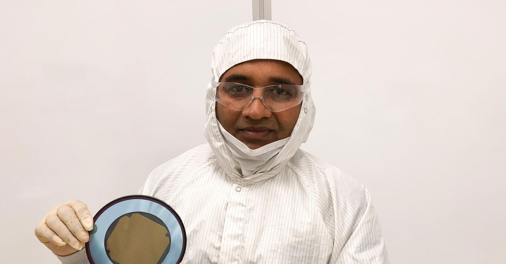
A 4-inch InP wafer of edge-emitting lasers for optical communications.
Sharing tools
At MACOM we are addressing every one of these weaknesses head-on by making our InP lasers on our 4-inch GaAs IC line with an etched-facet technology. By sharing existing equipment and infrastructure with that used for producing GaAs products, we not only reduce development costs, but also those associated with manufacturing, thanks to the sharing of fixed costs with other products.
Our etched facet technology has numerous advantages over its mechanical counterpart. Its greatest strength is that it is a high-volume production process – it enables on-wafer testing, with the pick-up of only good devices; and wafers do not have to be singulated to make bars and create a stack for facet coating. Another key attribute is that there is far greater freedom in the creation of the facet. No longer does it have to be made along a crystallographic angle of the wafer.
Figure 1. Ridge waveguide, edge-emitting lasers feature quantum wells for carrier confinement and cladding regions and ridges for optical confinement. Inserting the grating in the distributed feedback laser ensures single-mode output.
We produce our InP distributed feedback and Fabry-Pèrot lasers at our world-class GaAs IC fabrication facility, which is based in Lowell, MA. The facility is primarily used for manufacturing GaAs-based MMICs and GaAs/AlGaAs diodes, using the most cost-effective mainstream manufacturing process technologies.
Using high quality equipment that offers excellent process control, we have process modules for photolithography, implantation for isolation, metallization, dry/wet etch and back-side process. Photolithography is carried out using several high-quality steppers and e-beam writing tools, and the addition of ohmic and Schottky contacts are undertaken in multiple metallization systems, including those based on electron-beam and sputtering, using a variety of dome configurations. Our engineers also use: high-quality lift-off process tools and remote plasma cleaning process equipment to clean wafers and deliver defect-free devices; PECVD systems for the deposition of silicon nitride and silicon dioxide; and various dry etch tools, equipped with different gases, for etching semiconductor and dielectric layers. Our well established back-side processes include mounting, photo-processing with an infra-red mask aligner, grinding, polishing, back metal, dismount and cleaning. To monitor the processes and determine critical device dimensions, engineers turn to several high-end tools, including various scanning electron microscopes, automated optical inspection tools, optical and laser microscopes and profilometres.

Figure 2. Light intensity versus injection current for an MACOM 2.5 Gbit/s Fabry-Pèrot laser.
Adjusting this GaAs IC line so that it also produces InP lasers has not required substantial capital expenditure, because many of the existing tools can be used to manufacture photonic devices and control the production processes. Note that as well as keeping a close eye on the processing equipment, we use several in-line test systems, which can test process control monitor structures. This offers an insight into the health of the processes and the devices.
The lasers that we make emit at around either 1.55 µm, the sweet spot for low optical loss in a fibre, or 1.33 mm, where dispersion is minimum. For these wavelengths, various quaternaries can be used for the active region, but InGaAlAs is preferred in the quantum well, because it increases the speed of the laser and improves its high-temperature performance. Surrounding this layer are those made from the likes of InGaAs, InGaAsP, InGaAlAs and InAlAs – these are used to inject the carriers into the active region, confine them there, and control the optical modes within the chip.
Fortunately, there is much common ground between this set of materials and those used to make GaAs- based pHEMTs. The later are grown on semi-insulating GaAs, and primarily contain epitaxial layers of AlGaAs, InGaAs, InGaP and AlAs.
Figure 3. Emission spectrum showing different longitudinal modes from an MACOM Fabry-Pèrot laser at 25 °C. The injection current was about 28 mA
There are differences between lasers and pHEMTs, due to changes in composition required to ensure lattice-matching to either GaAs or InP substrates, and differences in dopants. For pHEMTs, the only dopant is silicon, while photonic structures may incorporate small amounts of silicon, zinc or boron.
However, it is the high degree of commonality between the two systems that allows many of the process modules used for the production of GaAs devices to also play a role in the manufacture of InP-based lasers. For example, both classes of device can be made using the same tools for photolithography, annealing, thinning and the addition of metal and dielectric layers.
Making lasers
Manufacture of our distributed feedback and Fabry-Pèrot lasers begins with the growth, by MOCVD, of heterostructures on 100 mm-diameter, n+ InP substrates. The structures contain a multi-quantum well active region, surrounded by graded-index separate confinement heterostructure layers, and a heavily doped, p-type InGaAs contact layer to improve the ohmic contact.
The high spectral purity of the distributed feedback lasers comes from the incorporation of a grating within the device. To form this, an InGaAsP layer is grown in the p-side of the structure. After the grating is created in this layer, regrowth takes place in an MOCVD chamber. The wafer is then removed and an oxide layer deposited, to form insulating pads underneath metal bond pads. Defining the facets and ridge follows, with different dimensions serving different applications. A p-type ohmic contact is then deposited on the ridge and on the oxide, a back metal is added on the n+ InP substrate, and the structure is then subjected to a rapid thermal anneal.
Figure 4. Box plot of the threshold current of 10 Gbit/s Fabry-Pèrot lasers on different wafers of multiple lots at 25 °C.
To modify the reflectivity of the facets, so that the device targets a particular application, we use different facet coating layers for our distributed feedback and Fabry-Pèrot lasers. After this, we test our lasers on-wafer at different temperatures. This includes an assessment of their most fundamental characteristics, revealed by the light output of the device as a function of injection current.
For our 2.5 Gbit/s Fabry-Pèrot lasers, measured at 25 °C, there are no kinks in the curve, indicating the absence of any instabilities in spatial and spectral modes (see Figure 2). Lasing begins at 8 mA, and the calibrated slope efficiency is around 0.48 mW/mA. The multiple longitudinal modes in the emission profile, centred around 1310 nm, are a characteristic of the Fabry-Pèrot architecture (see Figure 3).
Our portfolio of Fabry-Pèrot 1310 nm lasers also includes those that operate at 10 Gbit/s and have a threshold current of 6.5 mA. Measurements at 25 °C reveal that there is just a small variation in threshold current, which averages 6.5 mA. The variation in threshold current between wafers is small, indicating that the epitaxial wafers are of good quality, and there is little variation in the production process (see Figure 4).
To measure the on-wafer, small-signal optical modulation response at 25 °C, we have used the Anritsu VNA and O/E calibration module. This reveals an increase in bandwidth with injection current (see Figure 5). That’s primarily because cranking up the current increases the photon density within the cavity. Driven at 45 mA, bandwidth at the 3 dB point is about 15 GHz, which is well above the requirement for 10 Gbit/s operation.
Figure 5. Small-signal response of 10 Gbit/s Fabry-Pèrot lasers at 25 °C. The 3 dB bandwidth increases with injection current. It is about 15 GHz at 45 mA.
Figure 6. Single-mode spectrum of a 2.5 Gbit/s distributed feedback
laser observed at 25 °C. The side mode is suppressed by 46 dB. The
applied current was about 32 mA.
For our 1310 nm distributed feedback lasers, as expected, emission is
single mode (see Figure 6). The side-mode suppression ratio, defined as
the ratio of the power of the side mode to the main mode, is around 46
dB. This high value reflects the high degree of stability of the laser.
The small variation in wavelength of these devices, along with their
high side-mode suppression ratio, indicates that we have robust control
in our manufacturing process (see Figure 7). Operating at 25 °C, these
lasers have a threshold current of around 12 mA and a slope efficiency
of 0.47 mW/mA. These values are well within the range desired by
customers, and have enabled us to ship millions of 2.5 Gbits/s
distributed feedback lasers for GPON applications.
Figure 7. Box plot of emission wavelength of 2.5 Gbit/s distributed feedback laser on different wafers from multiple lots.
Successes with our 2.5 Gbit/s and 10 Gbit/s Fabry-Pèrot lasers and our 2.5 Gbit/s distributed feedback lasers have encouraged us to expand our portfolio with devices operating at higher speeds.
The key to increasing the speed of our distributed feedback lasers, and enabling them to operate at high temperatures, is to install a complex grating in the active layer. We will accomplish this with our existing equipment.
Production of these more complex lasers will need to replicate the approach we take with GaAs IC products. With those devices, the ohmic metal is deposited at the beginning of the flow, enabling the creation of process control monitoring structures. They allow in-line monitoring of electrical characteristics.
At present, the process control monitoring in place for laser production is not as sophisticated as this. There are process control monitors on the wafers, but they are only used for measuring etch depth, and the thicknesses of the oxide layer, metal, and facet coating layers. Verification of reflectivity and refractive index comes from separate monitors in the deposition system. What’s missing are structures for in-line electrical measurements that monitor contact resistance and diode characteristics. With the laser process flow, the metal layer is deposited at the end of the flow, so there is little benefit in process control monitoring at this point.
As we develop our technology for process control monitoring, we shall continue to refine our approach to high-volume manufacturing of InP lasers on our 4-inch GaAs line. Production costs for these chips will come down, driving up their deployment – maybe one day they’ll even be as widespread as the LED.


