
Imec Grows 2D Materials on 300mm Wafers
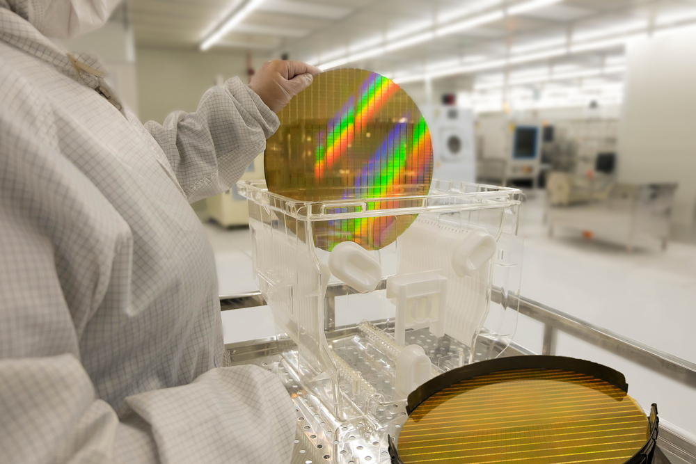
At the 2018 IEEE International Electron Devices Meeting (IEDM) in San Francisco (1 to 5th December 2018), Imec, the Belgian research and innovation hub, presented a 300mm-wafer platform for MOSFET devices using the 2D semiconductor WS2.
2D materials could provide the path towards extreme device-dimension scaling as they are atomically precise and suffer little from short channel effects. WS2 holds promise for higher ON current compared to most other 2D materials and good chemical stability.
Imec reported MOCVD growth, an approach that results in thickness control with monolayer precision over the full 300mm wafer and potentially highest mobility material. The benefits of the MOCVD growth come at the price of a high temperature while growing the material.
To build a device integration flow, the transfer of the channel material from a growth substrate to a device wafer is crucial. Imec is the first to demonstrate a full 300mm monolayer 2D material transfer, which is very challenging on its own because of the low adhesion of 2D materials to the device wafer and to the extreme thinness of the material transferred: 0.7nm. The transfer process was developed together with SUSS MicroTec and Brewer Science using temporary bonding and debonding technologies.
WS2 wafers are temporarily bonded to glass carrier wafers using a specially formulated material (Brewer Science). Next, the WS2 monolayer is mechanically debonded from the growth wafer and bonded again in vacuum to the device wafer. The carrier wafer is removed using laser debonding. This debonding technique is a key enabler for the controlled transfer of 2D materials
Iuliana Radu, Beyond CMOS program director at Imec, explains: “Building the 300mm platform for MOSFET device study with 2D materials and developing the process step ecosystem speeds-up the technological adoption of these materials. Several challenges are still to be resolved and are the subject of ongoing research and development.” Major challenges include scaling the equivalent oxide thickness (EOT) of gate dielectric for 2D materials, and reducing channel defectivity to boost mobility.
Imec’s research into advanced logic scaling is performed in cooperation with Imec’s key CMOS program partners including GlobalFoundries, Huawei, Intel, Micron, Qualcomm, Samsung, SK Hynix, Sony Semiconductor Solutions, TOSHIBA Memory, TSMC and Western Digital.


