
Balancing charges to boost performance
Incorporating a novel charge-balance drift region into a SiC Schottky barrier diode sets a benchmark for the key metric: on-resistance as a function of breakdown voltage
By ALEXANDER BOLOTNIKOV, REZA GHANDI, PETER LOSEE, STACEY KENNERLY AND RAVISEKHAR RAJU FROM GENERAL ELECTRIC
There are significant drawbacks associated with today’s medium-voltage power conversion systems. These converters – installed on ships, used in wind turbines, fitted on solar farms and appearing in traction drives in transportation – are held back by a maximum switching frequency of no more than several hundred hertz. This limitation, stemming from solid-state switch and diode losses, dictates that the transformer, as well as the components for the converter filter, are very large and heavy. In turn, this leads to high costs for the system and its installation, and restrains design flexibility.
What’s needed are highly efficient, lightweight power-conversion systems that can handle many megawatts while running at switching speeds of several kilohertz. Such converters are only a dream today, but they could become a reality if solid-state devices could switch at frequencies from one kilohertz to hundreds of kilohertz, while handling hundreds of amps.
GE is developing SiC Schottky barrier diodes with an impressive on-resistance for the given operating voltage
Those that are developing these devices include our team at General Electric. Our successes to date include a SiC junction barrier diode with a novel, charge-balanced architecture that slashes conduction losses.
The benchmark for judging our devices is the incumbent technology in medium-voltage power conversion applications: silicon insulated-gate bipolar transistors (IGBTs) and diodes made by the likes of Infineon Technologies and ABB. In these bipolar devices, injected carriers are stored in the device’s lightly doped blocking layers. In the on-state, these carriers increase the background carrier concentration, and enable a low forward-voltage drop (see Figure 1). And in the blocking-state, high voltages are possible, thanks to drift layers that are hundreds of microns thick and doped to levels of just 1013 cm-3. For silicon IGBTs, these layers can lead to a blocking voltage as high as 6.5 kV.
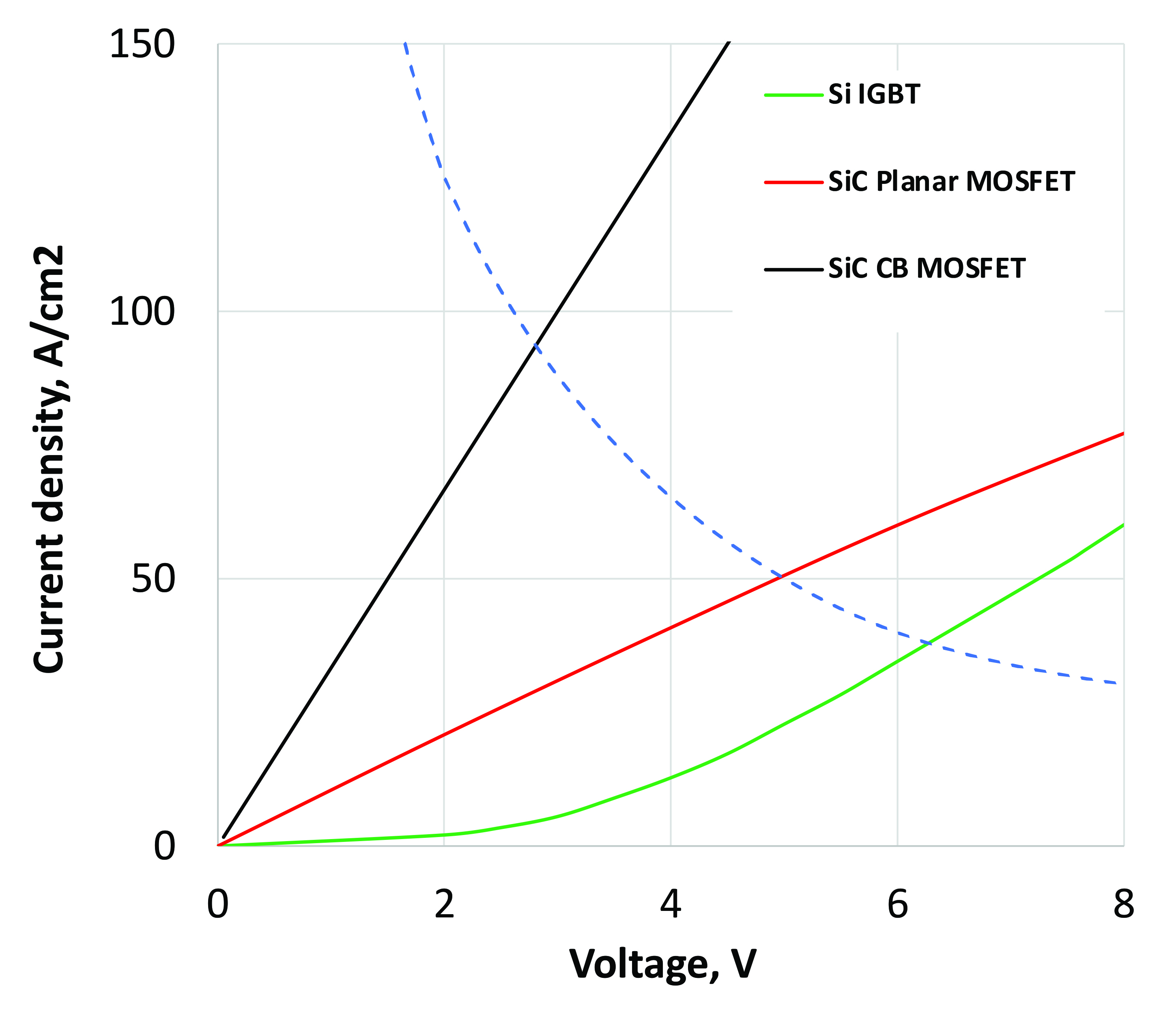
Figure 1. Comparison of typical forward characteristics of 6.5 kV devices at 125 °C. The SiC charge-balanced (CB) MOSFET offers a relatively high current density for a given forward voltage.
The penalty to pay for these stored carriers in high-voltage silicon power devices is extreme losses, even at switching speeds of just 1 kHz. Consider, for example, a silicon IGBT module designed to handle up to 6.5 kV and 400 A. It has a turn-off loss of 2.1 J, equating to 1 kW of dissipation for switching at 500 Hz.
Note that designers of these modules are not just trying to minimise this switching loss. Their overriding goal is to find the sweet spot between realizing low switching losses and a low conduction loss. So, for example, in modules made by ABB the on-state voltage ranges from 2.7 V to 5.4 V, well beyond the entitlement for a silicon turn-on voltage of 0.7 V. This high on-state voltage is chosen to ensure switching loss reduction, but it constrains current density to typically between 30 A/cm2 and 60 A/cm2.
Yet another limitation stems from the high on-state voltage drop associated with the bipolar devices’ p-n junction. This drags down converter efficiencies under partial load operation.
The solution to all these problems is to turn to wide bandgap power switches and diodes. Devices made from GaN and SiC promise far lower switching losses and more efficient power conversion in a wide range of applications. What’s more, for lower-voltage applications – that is those between 650 V and 2.5 kV – SiC devices also tend to operate with lower conduction losses.
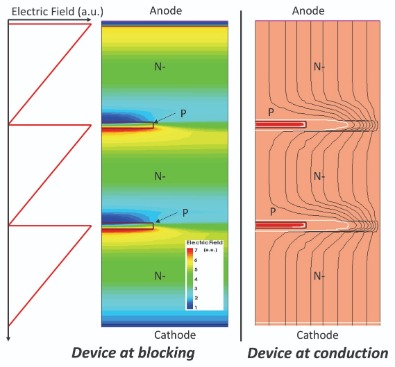
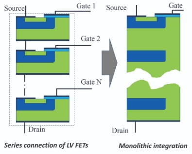
Figure 2. The operation (a) and design (b) of the charge-balance device.
However, when it comes to the devices typically deployed in medium-voltage converter applications, SiC is currently failing to fulfil its potential. One issue is that the conduction loss found in the drift layers of SiC unipolar devices is, at elevated temperature, often only marginally better than that of silicon IGBTs and diodes – and it can be even worse. Compounding matters, in SiC IGBTs, the large bandgap leads to an on-state voltage drop of more than 4 V at all operating current densities. And last but by no means least, the low current densities in SiC MOSFETs, IGBTs, and diodes results in the need for large die areas for handling the power levels required for megawatt applications. This is bad news, as it exacerbates chip costs.
Two options for addressing the decline in the performance of SiC devices at increasing voltages are the series connection of lower-voltage devices, and drift layer engineering that utilizes ‘superjunction’ technologies. The latter is preferred, as it does not require multiple devices. Instead, it features a drift/blocking region that consists of multiple, alternating n- and p-type doped pillars with a relatively high doping that allow a high breakdown voltage. This is in stark contrast to the standard approach for realising a high blocking voltage: a single, lowly and uniformly doped blocking region that when depleted results in a nearly uniform electric field distribution in the drift region.
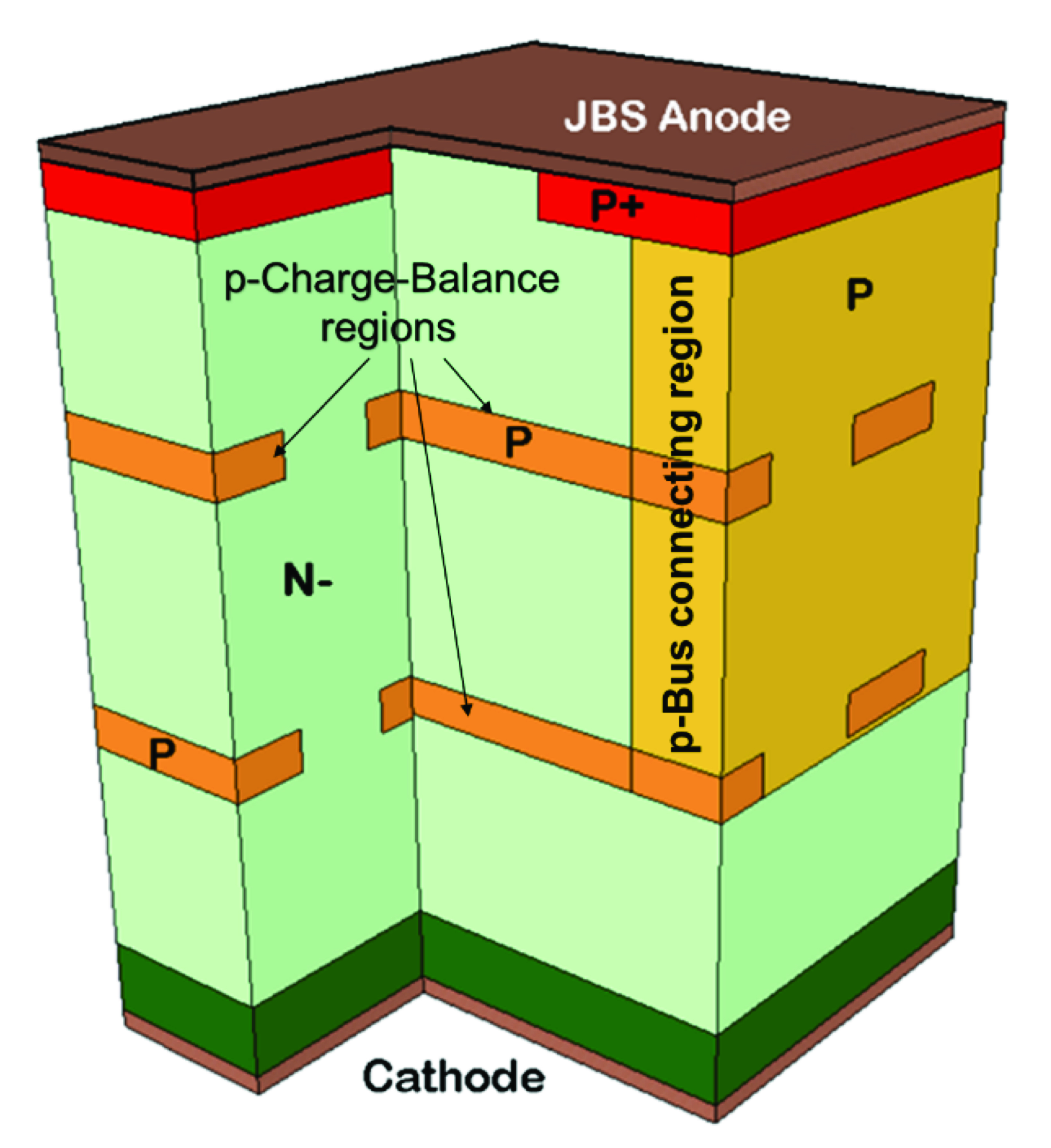
Figure 3. Engineers at General Electric are pioneering the SiC charge-balance junction-barrier Schottky diodes. They feature p-charge balance and p-connecting regions.
Several groups, including that headed by Paul Chow from Rensselaer Polytechnic Institute, have modelled the SiC superjunction vertical power device. But the realisation of these devices has remained elusive until now. While trench and refill approaches have garnered some interest, it is challenging to realise high aspect ratios, doping controllability, and scalability to higher voltages. These barriers have held back the experimental demonstration of a fully functional device.
We have broken through, by addressing the key challenge of achieving deep/high-aspect-ratio pillars of dopants in SiC superjunction devices with a novel, yet practical, SiC charge-balance drift region architecture. Armed with this technology, we have produced the first ever SiC junction-barrier Schottky diode.
How does charge-balancing work?
In our devices, the buried p-type charge-balance regions compensate for the higher n-drift doping concentration under reverse bias (see Figure 2). When the charge-balance regions are designed correctly, they act as electric field dividers, allowing an increase in doping in the drift region for a given breakdown voltage. The upshot is a reduction in conduction losses. Note that this concept is very similar to that of the serial connection of low-voltage devices that are monolithically integrated on the same chip.
The drawback of such a structure is its poor dynamic response. The charge-balance regions require holes in the n-type drift layer to transition from blocking to conduction. Unfortunately, this cannot occur quickly enough when relying only on the recombination-generation rates of the carriers. To alleviate this bottleneck, our design also employs p-Bus connecting highly doped p-type regions (p+) of the planar device to each of the charge-balance regions (see Figure 3). This refinement allows holes to flow into and out of the charge-balance regions during switching events.
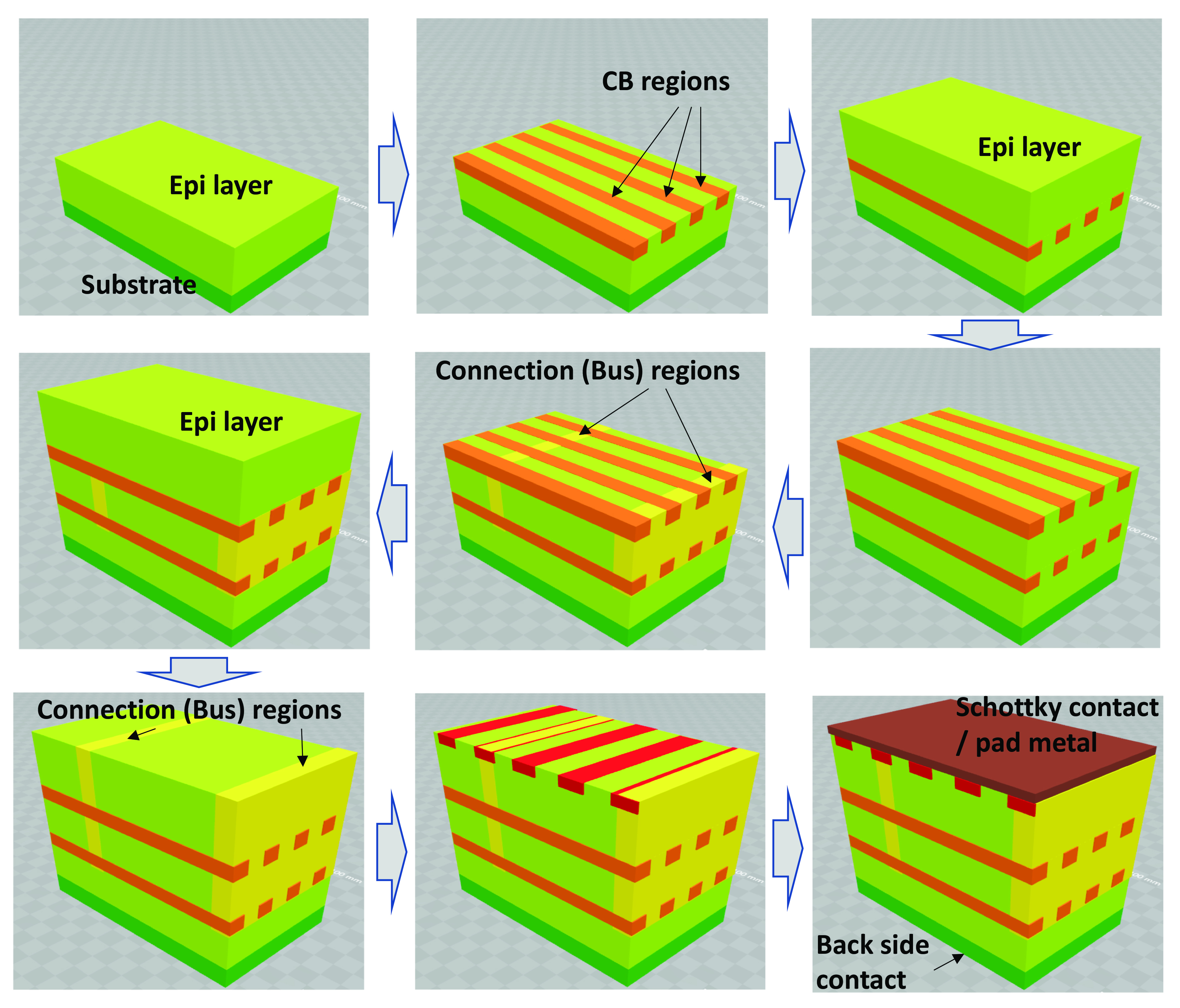
Figure 4. Several steps are required to fabricate SiC charge-balance junction-barrier Schottky diodes.
The challenge with our architecture is to make the p-Bus connecting region sufficiently narrow, and with low enough doping, to minimize the alteration of the electric field distribution of the charge-balance drift region; but to make this region conductive enough to establish a good connection between the p+ and charge-balance regions.
We have exceeded in this endeavour with our 2 kV and 3 kV SiC charge-balance, junction-barrier Schottky diodes, which were fabricated from 4H-SiC wafers with 10 µm-thick epitaxial layers doped at 1 x 1016 cm-3. Our fabrication process began with the formation of p-type charge-balance regions fabricated by ion implantation of aluminium. After this, we undertook additional epigrowth, before adding p-connecting regions via high-energy implantation of aluminium using Tandem Van de Graaff facility at Brookhaven National Lab.
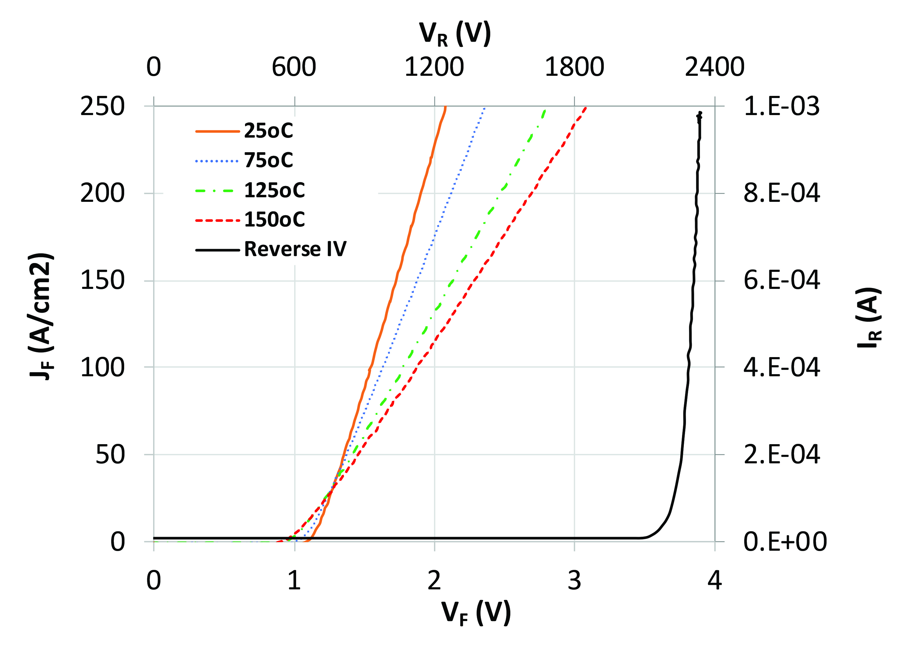
Figure 5. Forward and blocking current-voltage characteristics of a 2 kV SiC charge-balance junction-barrier Schottky diode.
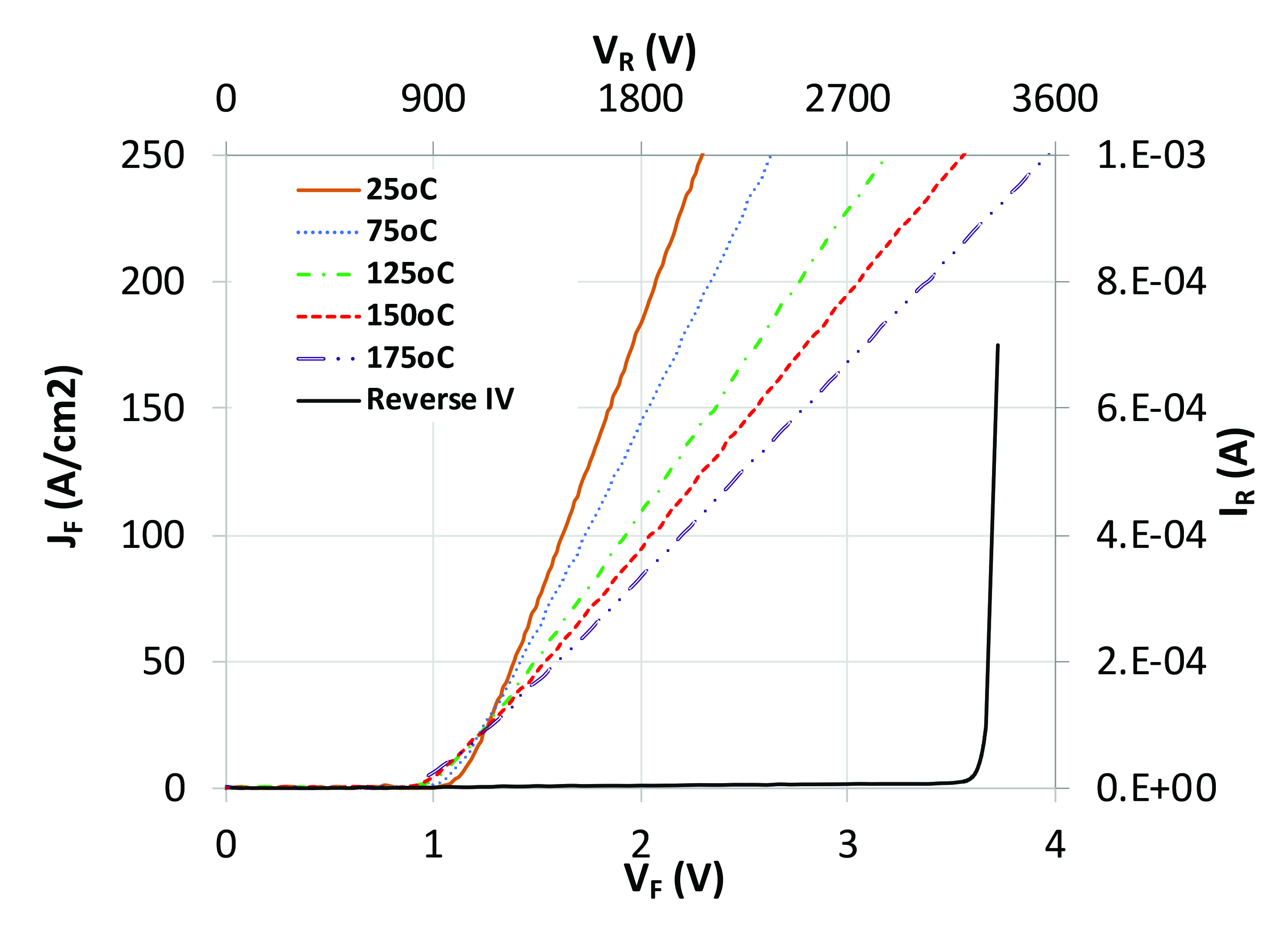
Figure 6. Forward and blocking current-voltage characteristics of 3 kV SiC charge-balance junction-barrier Schottky diodes.
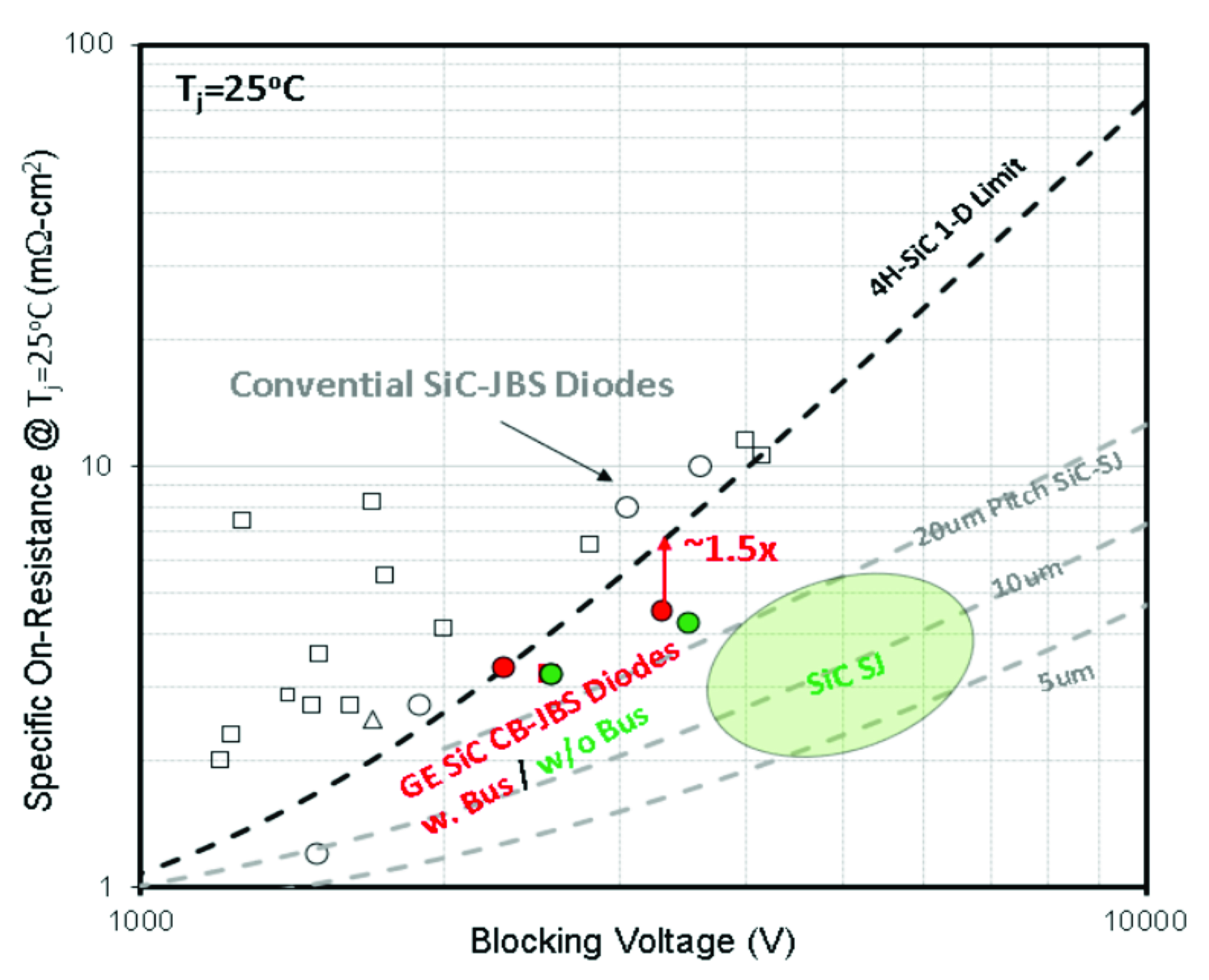
Figure 7. Differential on-resistance versus breakdown voltage for reported SiC FETs and diodes.
Our 2 kV diodes feature two 10 µm-thick epilayers and a single charge-balance region, while their 3 kV cousins have a total of three 10 µm epilayers and two charge-balance regions. Due to these differences, the steps for making 3 kV diodes include the fabrication of an additional charge-balance region, and further epitaxial growth and bus region implantation. In both cases, device fabrication is completed by forming a nickel-based Schottky junction-barrier diode on the top surface, and joining p+-regions to p-connecting regions.
After packaging these devices, we have tested them at both room temperature and elevated temperatures to evaluate their static and dynamic characteristics. Equipped with a nickel contact, the turn-on voltage for our diodes is around just 1 V (see Figures 5 and 6), while the differential room-temperature on-resistance is as low as 3.5 mΩ-cm2 and 4.3 mΩ-cm2 for the 2 kV and 3 kV versions, respectively. These measurements also uncover sharp breakdown voltages at more than 2.3 kV and 3.3 kV. Note that these values are far higher than would be possible with a conventional vertical device architecture sporting a drift layer doped at a concentration of 1 x 1016 cm-3.
We have compared the performance of our devices, both with and without connecting regions, to conventional SiC MOSFETs and diodes. Plotting the specific on-resistance as a function of blocking voltage revealed that at more than 3 kV, our devices outperform the theoretical one-dimensional unipolar limit by up to 50 percent, while the level of superiority over commercial devices is even higher (see Figure 7).
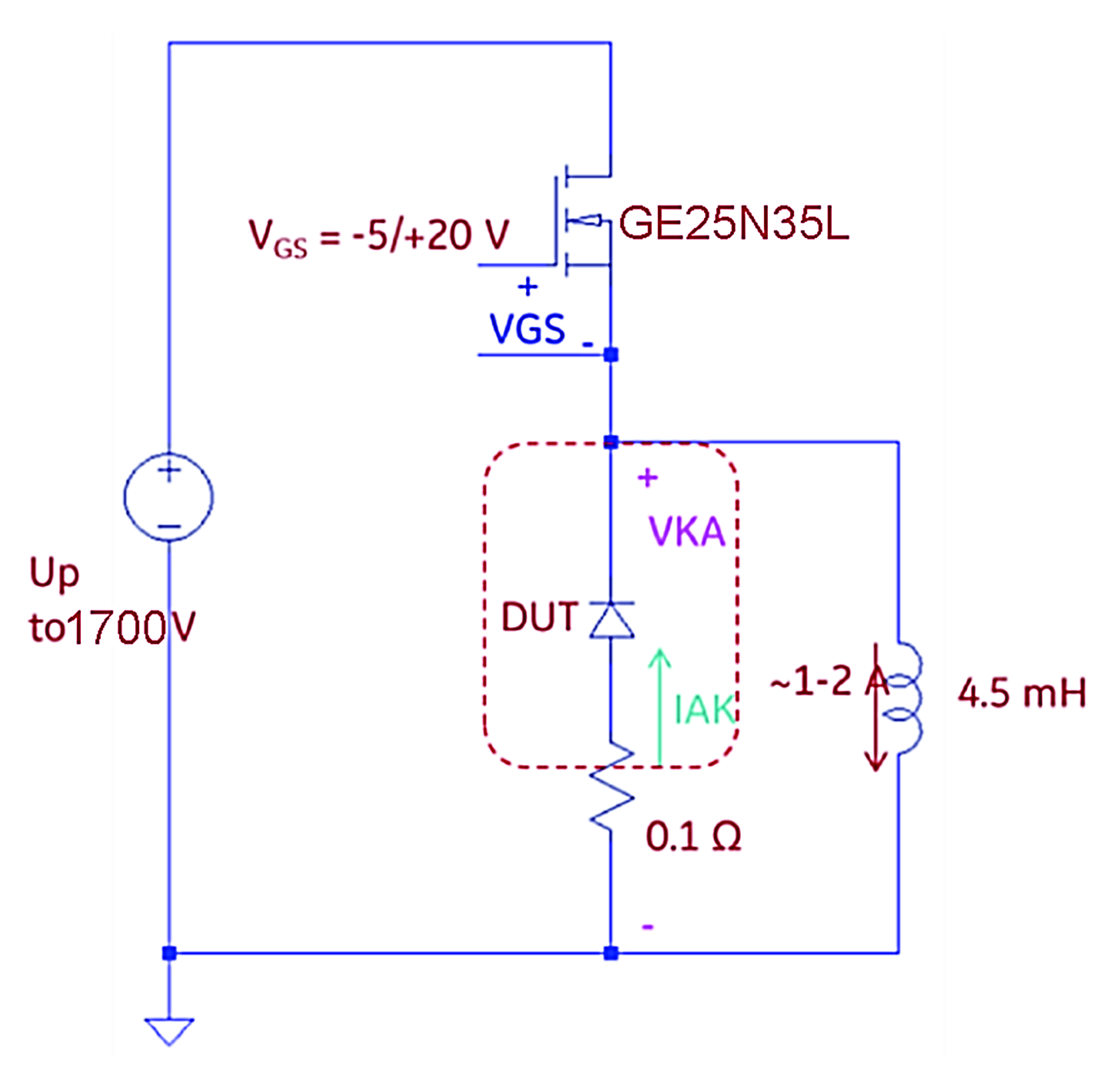
Figure 8. The high-voltage, double-pulse circuit used at General Electric to characterize its SiC charge-balance junction-barrier Schottky diodes assembled in TO-247 moulded packages.
Double-pulse switching tests have been used to assess the switching characteristics of our diodes (see Figure 8 for details of the circuit, which features the 2.5 kV/35 A SiC MOSFET, providing an active switch that is capable of turning on and off faster than 100 ns). Traces on an oscilloscope show that during the turn-on of the active switch there is reverse recovery in the charge-balanced junction-barrier Schottky diodes, followed by turn-on of the freewheeling diode during turn-off of the active switch.
These measurements enable us to estimate switching losses from forward recovery and reverse recovery of 12.91 mJ/cm2 and 1.9 mJ/cm2, respectively, for the 2 kV devices, and 23.65 mJ/cm2 and 2.49 mJ/cm2, respectively, for the 3 kV devices. For nominal conditions of a forward current of 125 A/cm2, a 50 percent duty cycle, and a junction temperature of 150 °C, total switching loss for a rated DC-link voltage is approximately 6.2 mJ/cm2 for the 2 kV device and 12.5 mJ/cm2 for the 3 kV device. Assuming a thermal limit of 250 W/cm2, these findings suggest that diodes could operate at frequencies of up to 20 kHz, and thus deliver a disruptive performance in many high-voltage power-conversion applications.
Our results show that SiC Schottky barrier diodes with a novel architecture featuring a charge-balanced drift region can break the one-dimensional limit for on-resistance as a function of breakdown voltage. This success should pave the way to medium-voltage-class SiC unipolar switches with on-state and dynamic losses that are well below those of their silicon counterparts. However, in order to capitalize on these benefits, there needs to be development of disruptive low-inductance and high-voltage packaging and converter topologies with improved thermal performance – and these technologies must accommodate the higher power densities and magnetics associated with the severe changes in voltage and current with time.
We will focus on scaling our developed, charge-balance device drift architecture to higher voltages. This has the potential to disrupt the existing units deployed in many applications that use switching frequencies of less than 1 kHz to more than 10 kHz. Look out for the next device we plan to demonstrate: a 4.5kV SiC charge-balanced MOSFET with a targeted room temperature specific on-resistance of less than 12 mW-cm2.
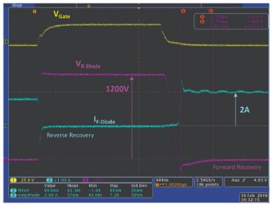
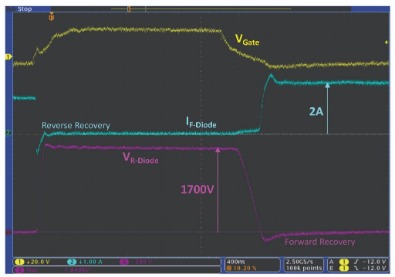
Figure 9. High-voltage double-pulse, diode-clamped inductive switching waveforms using a 2 kV (left) and 3 kV (right) charge-balance junction-barrier Schottky diode as the free-wheeling diode with reverse voltage of either 1200 V or 1700 V and a forward current of 2 A (forward current density is 250 A/cm2). The yellow trace represents the gate-source voltage of the MOSFET, used to turn-on the active switch and drive the freewheeling diode into reverse recovery until the diode current returns to zero and the load current flows through the switch. The reverse recovery phase of SiC charge-balance junction-barrier Schottky diodes is virtually indistinguishable from those of conventional SiC Schottky diodes. Beyond the reverse recovery phase, the reverse voltage on the charge-balance junction-barrier Schottky diode is 1200 V (left) and 1700 V (right) (these values are about 60 percent of the rated voltage). After some duration, the active switch is turned off and the load current begins to commute to the SiC charge-balance junction-barrier Schottky diode. With the active switch now in the off state, the forward current through the free-wheeling diode quickly ramps from zero to the full load current of 2 A. When turned on from blocking state to conducting state with a fast ramp, the SiC charge-balance junction-barrier Schottky diodes have an observable forward recovery phase. The waveforms show that the forward voltage across the diode has a large peak, before decaying back to nominal value for the forward voltage approximately 500 ns after turn-on. It is believed that this delay is due to the resistance from the p+ anode to the buried charge-balance regions via the deep p-bus regions. This view is consistent with a decrease of one-fifth in turn-on loss at 150 °C.
The information, data, or work presented herein was funded in part by the Advanced Research Projects Agency-Energy (ARPA-E), U.S. Department of Energy, under Award Number DE-AR0000674 advised by Program Director Isik Kizilyalli. The views and opinions of authors expressed herein do not necessarily state or reflect those of the United States Government or any agency thereof.
Further reading
F. Udrea et al. IEEE Trans. on Elec. Dev. 64 3 (2017)
L. Zhu et al. Journal of High Speed Electronics and Systems (2004)
L. Yu et al. IEEE TED Special Issue on SiC (2008)
K. Kojima et al. ECSCRM (2012)
L. Theolier MIEL, pp.79 - 82 (2010)
J. Nishio et al. IEEE Trans. on Elec. Dev. 55 1954 (2008)
A.Bolotnikov US20170278924A1 (2016)
R. Ghandi et al. Mat. Sci. Forum 924 573 (2017)


