
Superior silicon carbide
Solution growth eliminates basal plane dislocations in high-quality single crystals of bulk SiC
BY KAZUHIKO Kusunoki, KAZUAKI Seki and YUTAKA Kishida from Nippon Steel AND Sumitomo Metal Corporation and HiRONORI Daikoku, HIROAKI Saito, ISAO Kobayashi and HIROSHI Mihara from Toyota Motor Corporation
The global demand for electricity is rising far faster than that for all forms of energy. According to the International Energy Agency, worldwide energy demand increased by 2.1 percent in 2017, while that for electricity climbed by 3.1 percent.
As electricity usage rises, the total gains resulting from more efficient power devices will become ever more significant. This makes it more attractive than ever for humanity to invest in SiC diodes and transistors, which have much lower losses than their silicon siblings.
Right now, sales of SiC devices are climbing fast. But even more success is possible, along with a greater share of the power semiconductor market, if SiC manufacture were to include the production of substrates that are cheaper, larger, and exhibit a higher crystal quality. Read on to discover how this can be accomplished.
Growing single crystals of SiC is far from easy. The 4H-SiC single crystal substrates that are on the market today are plagued by various dislocations – in total, the density of imperfections is in the range of thousands to ten thousand per cm2 (see Table 1 for a list of common dislocations, and Figure 1 for an illustration of how they may appear in 4H-SiC single-crystal substrates). These dislocations are a menace, driving down device manufacturing yield and applying the breaks to far greater deployment of SiC power devices.
By far the most troublesome class of dislocations are the line defects in the 4H-SiC{0001} basal planes. Known as basal plane dislocations, these killer defects wreak havoc with device performance. It drops when a forward voltage is applied across 4H SiC MOSFETs and p-i-n diodes, and basal plane dislocations are driven from the SiC single-crystal substrates to the epitaxial layers, where they expand and turn into Shockley-type stacking faults. There they act as high-resistance layers, increasing the on-state voltage and driving a deterioration in device performance.
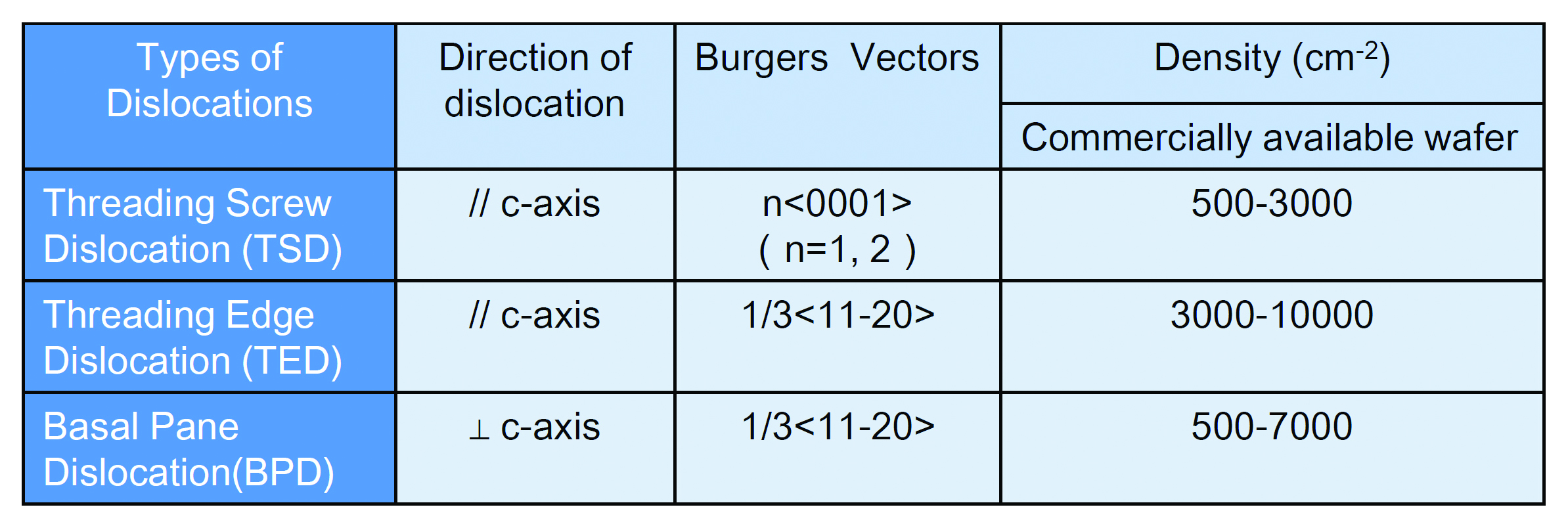
Table 1. Types and density of dislocations in 4H-SiC crystals
One way to address this issue is to convert the basal plane dislocations into threading-edge dislocations at the interface between the epitaxial stack and the substrate. This conversion must take place during the epitaxial growth, by CVD, of layers on the SiC substrate. Note that the threading-edge dislocations that are formed are harmless, as they don’t degrade device characteristics. However, as it is not possible to convert every single basal plane dislocation into a threading-edge dislocation, this is an imperfect solution. It would be far better to completely eliminate the basal plane dislocations in SiC.Unfortunately, it is challenging to produce SiC crystals, the starting point for substrate production. At normal pressure, there is no liquid phase of SiC with a chemical composition for the melt that matches that of the solid state. Consequently, it is theoretically impossible to carry out melt growth by solidification, which is the approach adopted for making silicon boules.
Due to this limitation, today’s SiC substrates are manufactured with a gas phase method that can produce 4H-SiC bulk single crystals. Sublimation takes place at temperatures of at least 2,300 °C. Stresses associated with the high temperatures, and cooling down from them, give rise to thermal stress. This is released by movement in 4H-SiC basal planes, which are easy slip planes, and results in basal plane dislocations with a density of hundreds per cm2 or more.
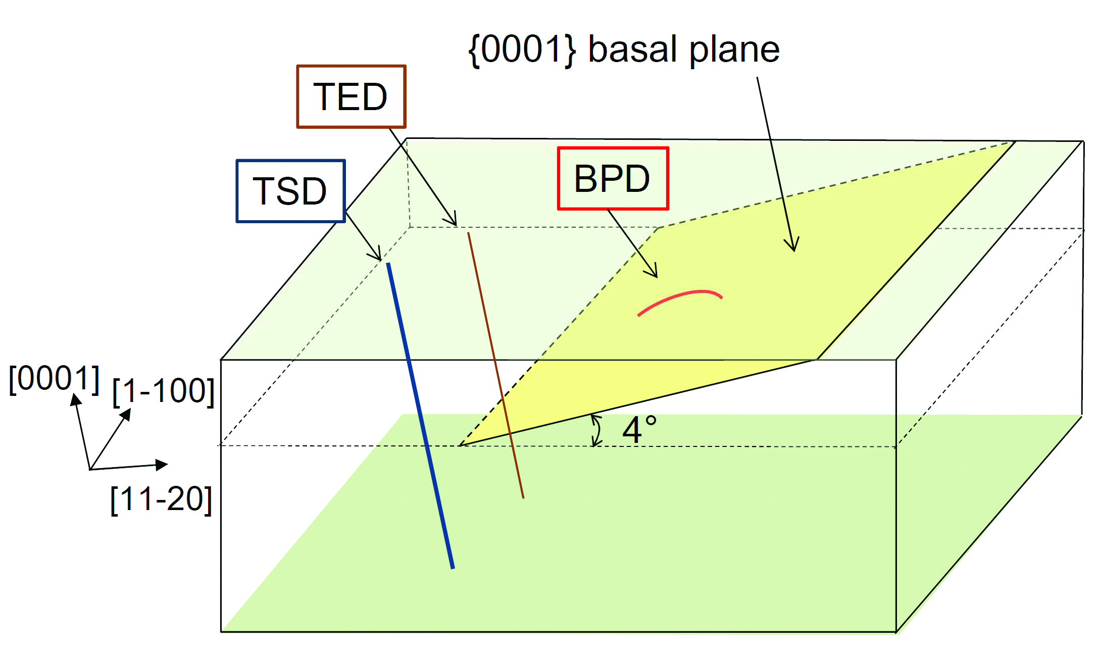
Figure 1. Dislocations in a 4H-SiC single crystal substrate (4° off-axis)
The highest quality crystals formed by the sublimation method are those that have been made by a team from Toyota Central R&D Labs, Japan, using repeated a-face (RAF) growth. However, this material is not free from basal plane dislocations.To eradicate these dislocations, an alternative growth method is required. That’s the approach that our team from Nippon Steel and Sumitomo Metal Corporation and Toyota Motor Corporation is taking, using a solution growth technique to realise ultra-high-quality SiC single crystals.
Our approach is a form of liquid phase growth. SiC is dissolved in a metallic melt that contains chromium or titanium, with supersaturation driving the formation of the crystal. With this approach, the reaction takes place at close to the thermodynamic equilibrium state, enabling the crystal growth to proceed at a temperature that is lower, by a few hundred degrees Celsius, than it would be for a sublimation method (see Figure 2).
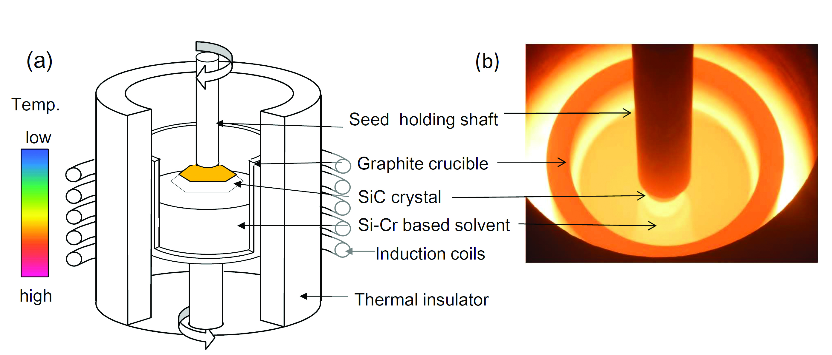
Figure 2. (a) The SiC solution growth set-up used by engineers at Nippon Steel and Sumitomo Metal Corporation and Toyota Motor Corporation. The graphite crucible, which provides a container for the solvent and a carbon source, is directly heated by induction. Growth, typically at 2000°C, is conducted under atmospheric pressure in a mixture of helium and nitrogen gases. (b) Inside a crystal growth furnace.
Suppressing solvent inclusionsOne of the challenges with our approach is that as the SiC crystal forms from a liquid phase, we must prevent the surface from roughening as the material thickens. This threat, known as surface morphology instability, can create concavities and convexities with dimensions of several hundred microns to several millimetres. In the fine concavities, any solvent microdrops that are left can spawn macroscopic defects, known as solvent inclusion.
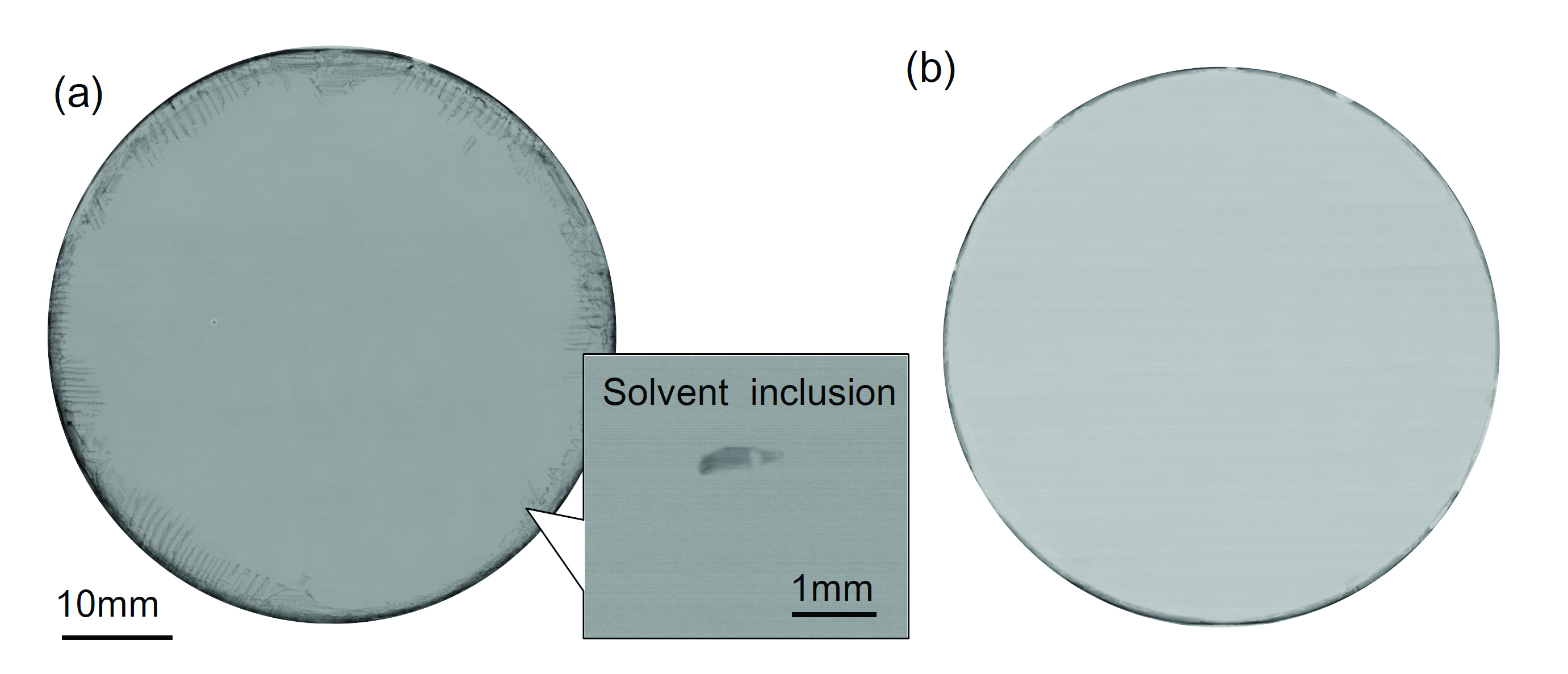
Figure 3. Transmission X-ray images of 2-inch-diameter 4H-SiC ingots (a) before optimising crystal growth conditions, and (b) after optimisation. It is clear that several dark domains exist at the peripheral part on the crystal, formed using the conventional growth technique. These domains are ascribed to a metal solvent that has a lower X-ray transmittance compared with the SiC matrix. Note that no dark domains are observed for the whole volume in the crystal after optimising growth conditions, indicating that this material is free from solvent inclusion.
Substrates with this form of imperfection are unsuitable for making power devices. So, to prevent them forming, the growing surface has to be smooth for extended periods of time during crystal growth. That’s a very demanding technical challenge that has remained elusive for many years.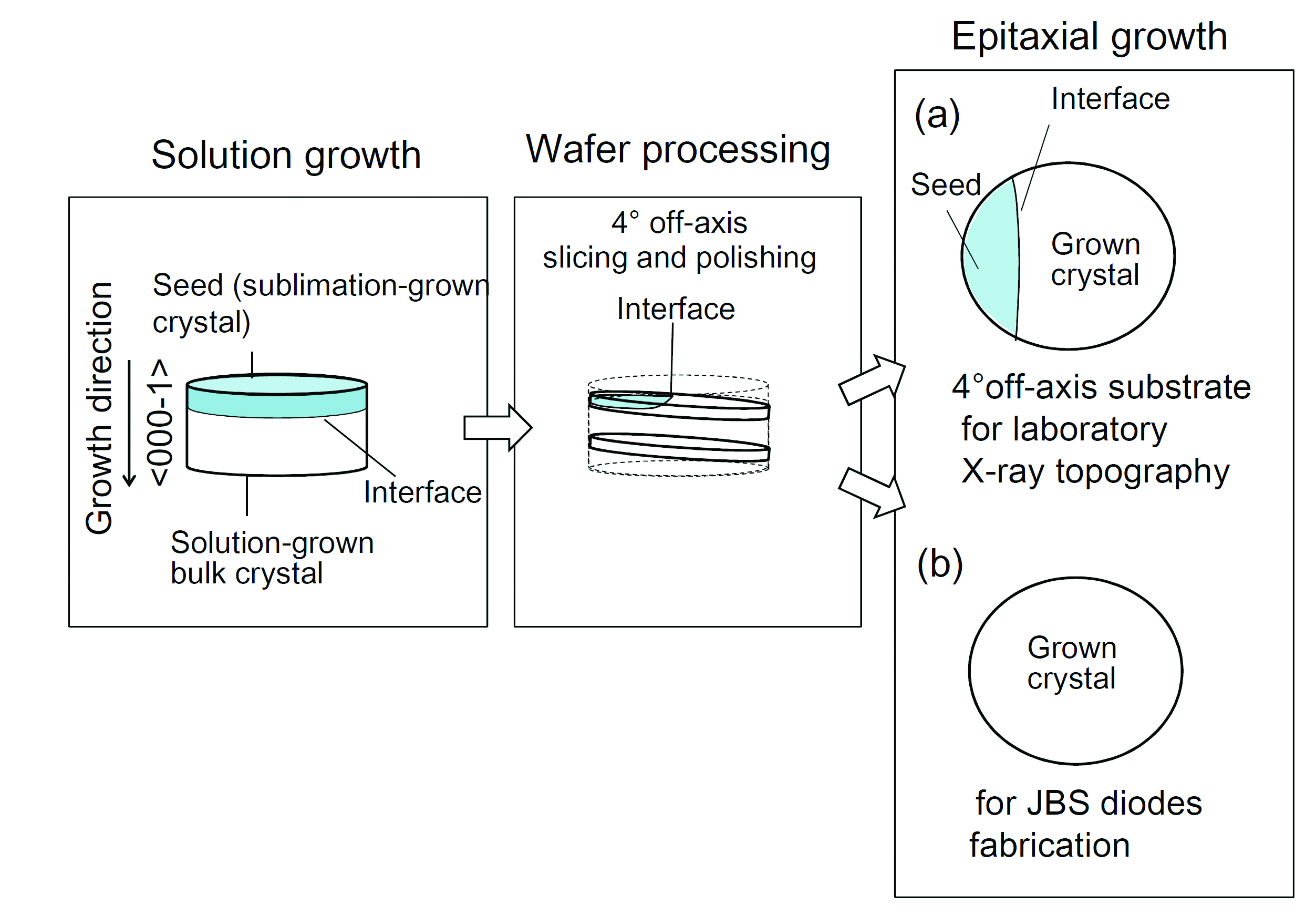
Figure 4. Slicing the material produced by the solution growth method creates (a) wafers for evaluating dislocations, and (b) wafers for prototyping junction barrier Schottky diodes.
We have overcome this challenge by considering the numerous process factors associated with crystal growth. Taking this approach reveals that it is possible to stabilise the surface morphology, and ensure a smooth surface, by controlling the growing interface outline while suppressing changes in supersaturation over time. By adopting these findings, we have produced the first 2-inch bulk crystals that are free from solvent inclusion (see Figure 3).Using the solution growth method, we have also produced 4-inch crystals that are more than 10 µm-thick. An obvious next step is to apply the solvent inclusion elimination technology that we have established for 2-inch diameter crystals to the growth of those that are 4-inch in diameter.
Those of us at Nippon Steel and Sumitomo Metal Corporation are drawing on this growth technology to produce, from ingots, 2-inch diameter 4H-SiC substrates with an off-angle of 4°. These can provide a great foundation for making for power devices.
To evaluate the quality of our SiC substrates, we have compared the dislocation density of our crystals produced by the solution growth method – from now on referred to as solution-grown crystals – with that of a seed crystal. This has been accomplished by using the solution growth method to grow a crystal on the on-axis plane (0001) of a seed crystal. Tilting this at 4°, and slicing and polishing wafers from it, creates a sample that includes the interface between the seed crystal and solution-grown crystal.
We deposited a 10 µm-thick layer on this sample by CVD, before scrutinising the material with X-ray topography (see Figure 4). This reveals that the seed crystal area features a high-density mesh contrast, originating from basal plane dislocations. Meanwhile, in the solution-grown crystal area, no such contrast is observed.
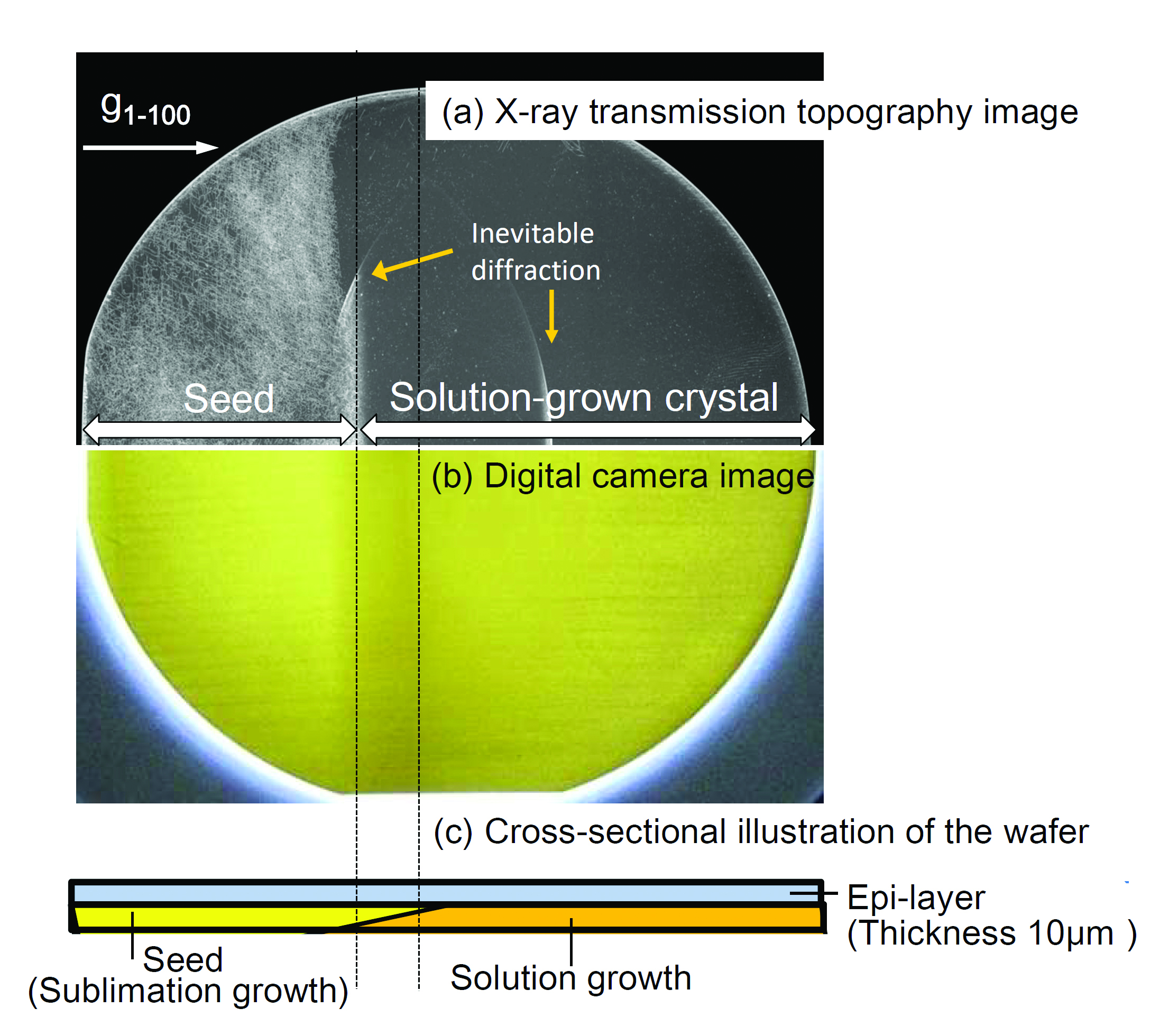
Figure 5. 2-inch diameter 4H-SiC wafers have been analysed by (a) transmission X-ray topography, (b) digital camera images, and (c) by taking cross-sections.
These findings indicate that there are no basal plane dislocations in the solution-grown crystal (see Figure 5). In addition, they show that when the basal plane dislocations in a seed crystal in the {0001} plane intersect at right angles with the crystal growth direction, they do not propagate into the solution-grown crystal. Yet another insight provided by X-ray topography is that the solution growth and cooling processes do not generate any new basal plane dislocations. We attribute this to the lower temperature for solution growth than for sublimation growth.To ensure high-performance devices, the surface of SiC must be impeccably clean. This includes incredibly low levels for metallic contaminants on the surface, as their presence can degrade the characteristics of a power device, and compromise yield.
As our solution growth involves a chromic solvent, there is a danger that this might impair the quality of our material. To see if that is the case, we have quantified the metallic impurities on the front and back sides of our of epitaxial wafers, using inductively coupled plasma mass spectrometry and direct acid droplet decomposition.
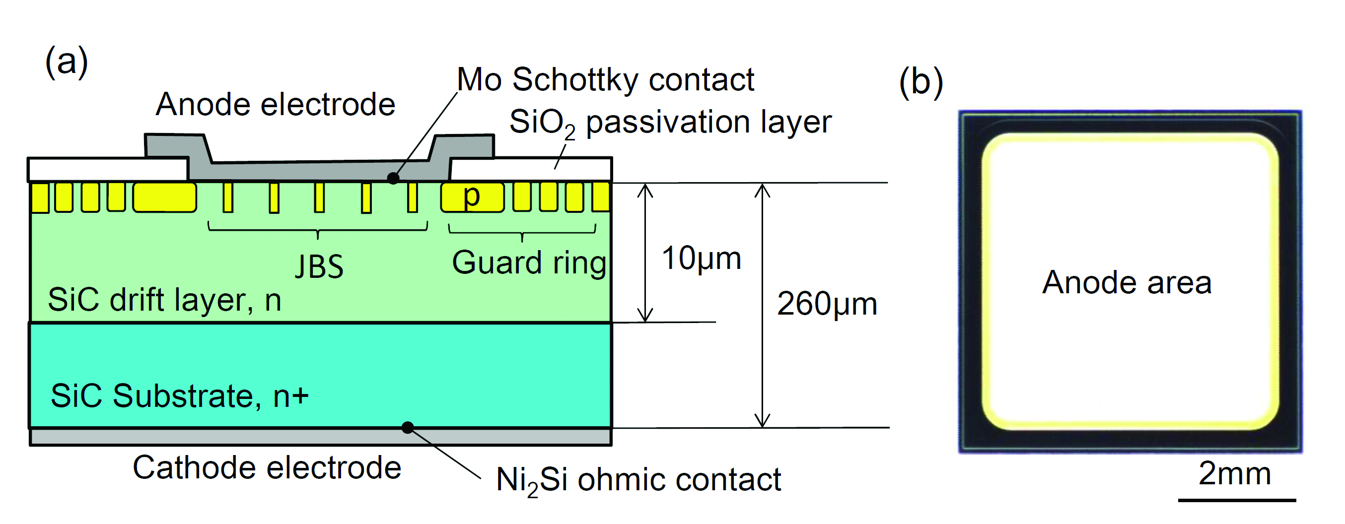
Figure 6. (a) A vertical cross-sectional view of junction barrier Schottky diode. (Taken from H. Fujiwara et al. Appl. Phys. Lett. 100 242102 (2012). (b) Plan view of a junction barrier Schottky diode. Active area is 6 mm by 6 mm.
This technique reveals that the front and back sides of our wafers have negligible levels for many common metals – values were below 3.5 × 10¹¹ atoms/cm2 for more than a dozen common elements: calcium, sodium, potassium, magnesium, titanium, chromium, manganese, iron, cobalt, nickel, copper, zinc and aluminium. We believe that the extreme cleanliness of the surfaces of our solution-grown SiC wafers could result from the availability of bulk crystals without solvent inclusion. Such low levels of contaminants confirm that there are no concerns associated with using solution-grown SiC epitaxial wafers in device manufacturing lines.Building better devices
We have fabricated the world’s first junction-barrier Schottky diodes at the wafer level on solution-grown SiC. For the production of these devices, we used a 2-inch diameter solution-grown 4H-SiC substrate (see Figure 6).
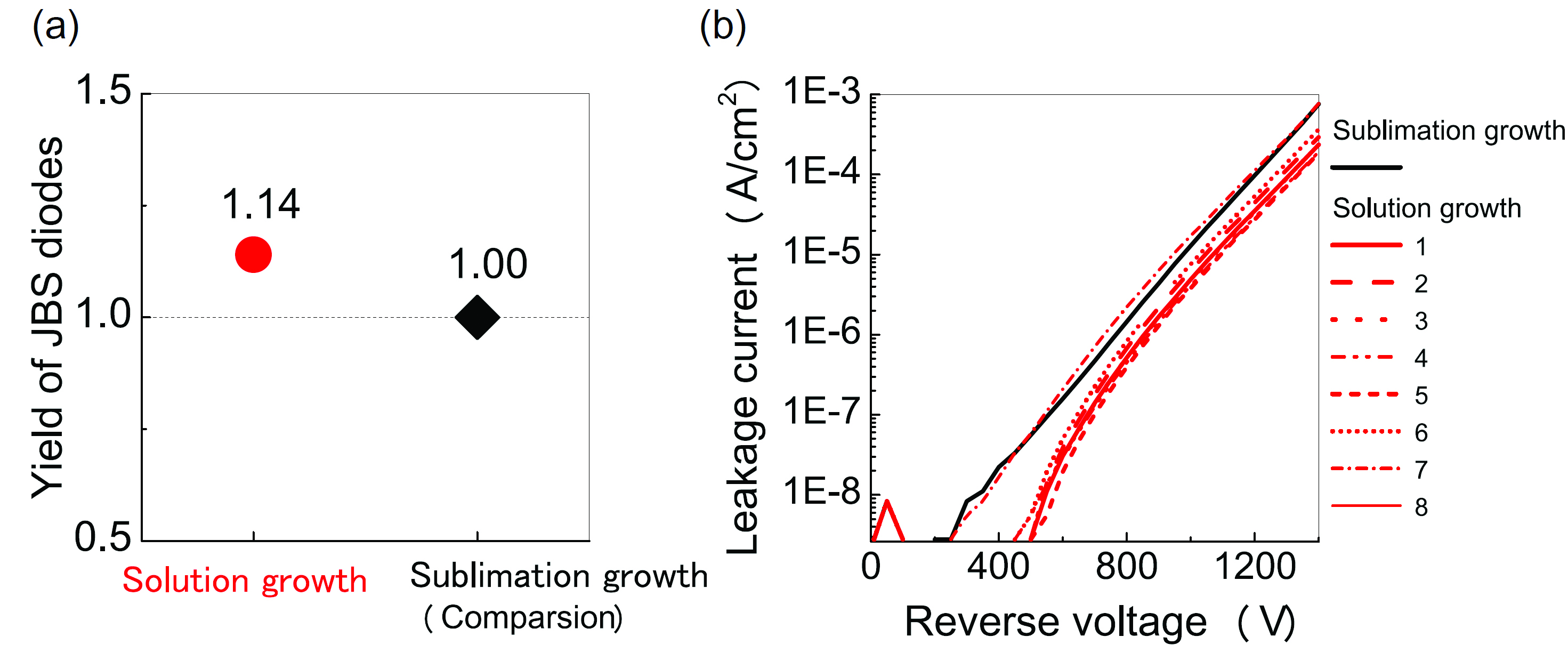
Figure 7. (a) A comparison of the proportion of efficient junction-barrier Schottky diodes fabricated on solution-grown and sublimation-grown SiC substrates. Note that the yield of the junction-barrier Schottky diodes fabricated on the solution growth substrate was normalized by that obtained on the sublimation-grown substrate. (b) Relationship between reverse current and voltage characteristics for the junction barrier Schottky diode.
To evaluate the electrical performance of the diodes, we compared their performance with equivalents grown on commercially available, high-grade substrates manufactured by sublimation. The efficiency and electric characteristics of devices grown on our substrates are equal to, or higher than, those grown on the alternative foundation (see Figure 7).This test is not ideal for highlighting the superiority of our substrates. That’s because basal plane dislocations in the substrate have little effect on the degradation of electric characteristics of a junction barrier Schottky diode. Where our substrates promise to make a far bigger contribution is to improving the performance of diode-built-in MOSFETs and 4H-SiC p-i-n diodes. When prototypes of these devices are made on our substrates, they will demonstrate the overwhelming superiority of solution-grown SiC crystals.
We have made much progress, but there is still work to do. Today, sublimation is used for high-volume manufacture of 6-inch diameter SiC, while the diameter of solution-grown wafers is still small, delaying success in the marketplace.
However, when solution grown SiC material hits the market, success could be rapid. This form of substrate will be in much demand, thanks to its absence of basal plane dislocations, a known killer defect that is an obstacle to obtaining high-performance, highly-reliable SiC power devices. What’s more, for this form of substrate, costs have the potential to fall below those made by sublimation, as growth takes place at normal pressure and under lower temperatures.
Further reading
H. Daikoku et al. Cryst. Growth Des. 16 1256-1260 (2016)
K. Kusunoki et al. Mater. Sci. Forum 924 31 (2018)
K. Seki et al. Mater. Sci. Forum 924 39 (2018)
K. Kusunoki et al. to be published in Mater. Sci. Forum (2019)


