

Unleashing the promise of gallium oxide

Gallium oxide Schottky barrier diodes
incorporating narrow trenches are setting new benchmarks for voltage
blocking and leakage current BY WENSHEN
LI, ZONGYANG HU, KAZUKI NOMOTO, DEBDEEP JENA AND HUILI GRACE XING FROM
CORNELL UNIVERSITY
Gallium oxide Schottky barrier diodes incorporating narrow trenches are setting new benchmarks for voltage blocking and leakage current
BY WENSHEN LI, ZONGYANG HU, KAZUKI NOMOTO, DEBDEEP JENA AND HUILI GRACE XING FROM CORNELL UNIVERSITYIt’s of little surprise that there has been a consistent drive toward the use of wider bandgap materials for power electronics. After all, the wider the bandgap, the greater the breakdown field, opening the door to making devices with a higher breakdown voltage for the same material thickness.
However, nature is not always that generous. Typically, a move to a wider bandgap is accompanied by more challenging doping, along with difficulty in making high-quality native substrates. Judged in these terms, gallium oxide appears to offer a sweet spot beyond SiC and GaN.
One of the most promising forms of gallium oxide is its b-phase, which has a bandgap of 4.5-4.7 eV. Luckily, it is easy to dope this oxide n-type in a controllable manner, to realise doping that spans 1015 cm-3 to 1020 cm-3. Thanks to shallow donor levels throughout this range, doping efficiency is high at room temperature. Another encouraging aspect of Ga2O3 is that single-crystal substrates of this material can be readily produced with melt-growth techniques, mirroring the manufacture of those made from silicon. Given all this promise, is it possible to harvest all the benefits arising from the large bandgap of Ga2O3 and demonstrate devices that are superior to those made from SiC and GaN?
To help answer this question, our team at Cornell University has been focusing on the development of Ga2O3 vertical power devices. By employing a vertical topology, they are capable of carrying more current per chip area, while taking advantage of the readily available Ga2O3 single-crystal substrates. Our goal is to demonstrate the highest unipolar performance that Ga2O3 can deliver – it is projected to be far higher than that of SiC and GaN, primarily due to a leap in the breakdown field to 6-8 MV/cm, arising from the superior bandgap.

A judicious junction
A drawback of Ga2O3 is its lack of p-type doping.
Due to this drawback, we incorporate metal-insulator-semiconductor (MIS) junctions in our devices to enhance their blocking voltages. As we’re about to see, the reason behind using of this form of junction is far from trivial.
Let us begin by considering a MIS structure under reverse bias: the semiconductor enters deep depletion near the junction, and a so-called inversion layer results, due to thermal energy within the device promoting electrons from the valence band to the conduction band. This is not good news, as once the inversion layer is created, the entire reverse bias is dropped across the insulator of the MIS structure, leading to catastrophic failure of the insulator and thus the power device. The only option for preventing this catastrophe from taking place is to evacuate the resulting minority carriers quickly. In our case, that means evacuating the holes in an n-type semiconductor.
A key figure-of-merit in this process is the time constant associated with the inversion process (as can be seen in Figure 1, this characteristic is governed by the bandgap).
For semiconductors with a small-bandgap, such as silicon and GaAs, at room temperature an inversion layer forms within seconds or minutes; and at elevated temperatures, where a power device often operates, this time is far shorter, as the time constant plummets by several orders of magnitude. So, in silicon and GaAs devices, a proper p-type contact is needed to sweep out the holes that are generated by either thermal generation or impact ionization.
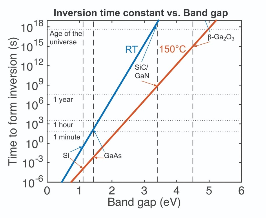
Figure 1. The estimated inversion time constant in MIS-junctions as a function of the bandgap. The time to form the inversion layer increases exponentially with increasing bandgap, allowing for the use of a MIS-junction for voltage blocking in wide bandgap semiconductors without the concern for MIS-junction snapback with time. Or, to view this graph from another perspective, there is a necessity to employ p-type contacts in narrow bandgap semiconductors, but they can be avoided in wide bandgap semiconductors.
In sharp contrast, there is almost never any need to worry about evacuating holes out of Ga2O3, so long as the semiconductor is sufficiently pure, and no optical absorption or impact ionization takes place to generate holes. Armed with a sizable bandgap of around 4.5-4.7 eV, Ga2O3 effectively suppresses the formation of an inversion layer; and devices made from this oxide will be packaged, preventing absorption of external light.In fact, for Ga2O3, the electric field required for impact ionisation is so high that it can hardly be supported by a true insulator. Even if impact ionisation happens, the generated holes are highly localized, due to the polaron effect and the super flat valence band. This makes it very difficult to evacuate these holes, and the best way forward is to suppress their formation in the first place.
Based on the arguments that we have just presented, we are pursuing an architecture that employs a MIS-junction for voltage blocking and avoids a p-n junction. The significance of the time constant associated with inversion layer formation in a MIS structure is not widely known. However, it is another important virtue of wide bandgap and ultra-wide bandgap semiconductors.
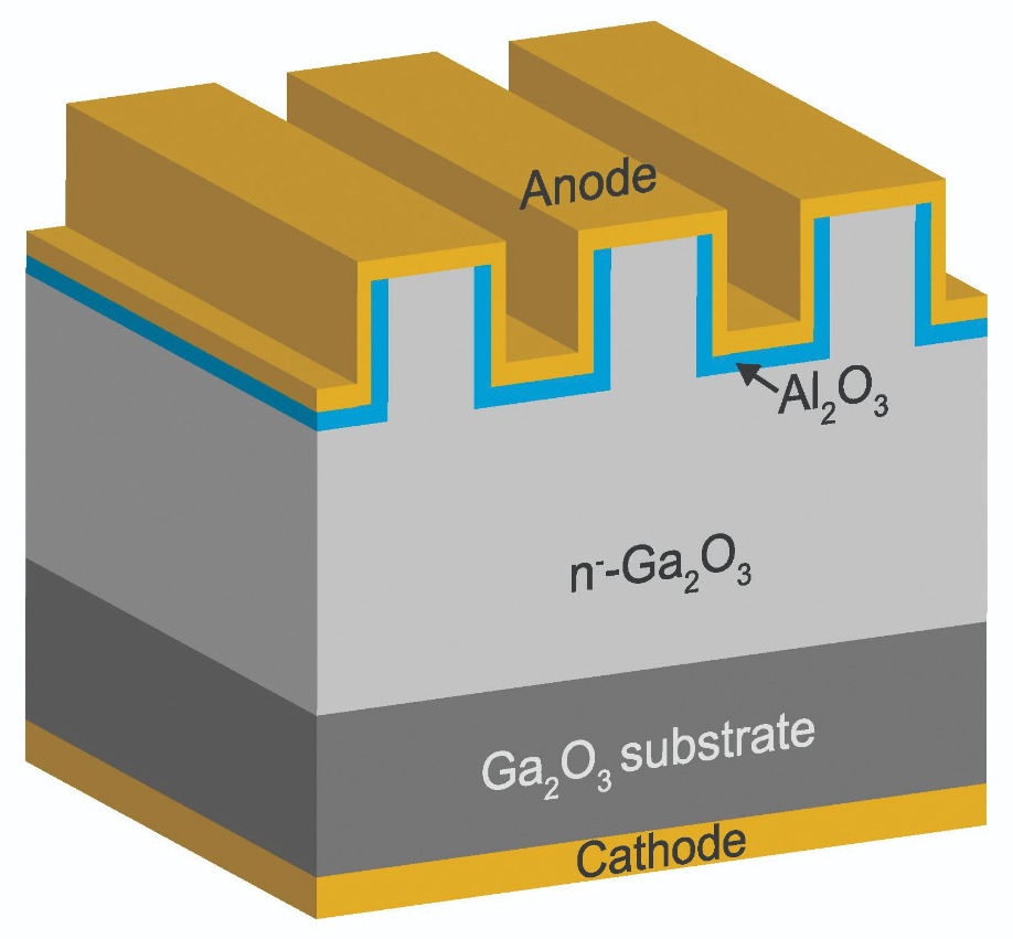
Figure 2. The Ga2O3 trench-MIS Schottky barrier diode features a periodic fin channel, formed by etched trenches. MIS-junctions covering the trenches provide a charge-coupling mechanism that effectively reduces the electric field near the top Schottky contact.
Adding trenchesWe have focused our efforts on the development of a Schottky barrier diode. This device is capable of a fast switching speed, due to unipolar operation, but it is compromised by a lower breakdown voltage and a higher leakage current. To address both of these drawbacks, we engineer a charge-coupling mechanism around the Schottky contact. The result: a trench-MIS barrier Schottky diode (see Figure 2), a device that effectively reduces the electric field near the top Schottky contact.
Simulations of a form of our devices, which has a fin channel width of 1 µm and a trench depth of 1.5 µm, reveal the electric field profile when the diode is blocking 2.44 kV – this is the highest breakdown voltage we have achieved so far. According to these calculations, the charge-coupling mechanism reduces the electric field near the Schottky contact to below 1 MV/cm. Due to the trench structure, termination of the electric field is predominantly to the metal at the sidewall, rather than to the top Schottky metal. In contrast, in a regular Schottky barrier diode that does not gain the benefit of the charge-coupling effect, the surface electric field is 4 MV/cm. This value is so high that it leads to an unacceptably-high leakage current density.
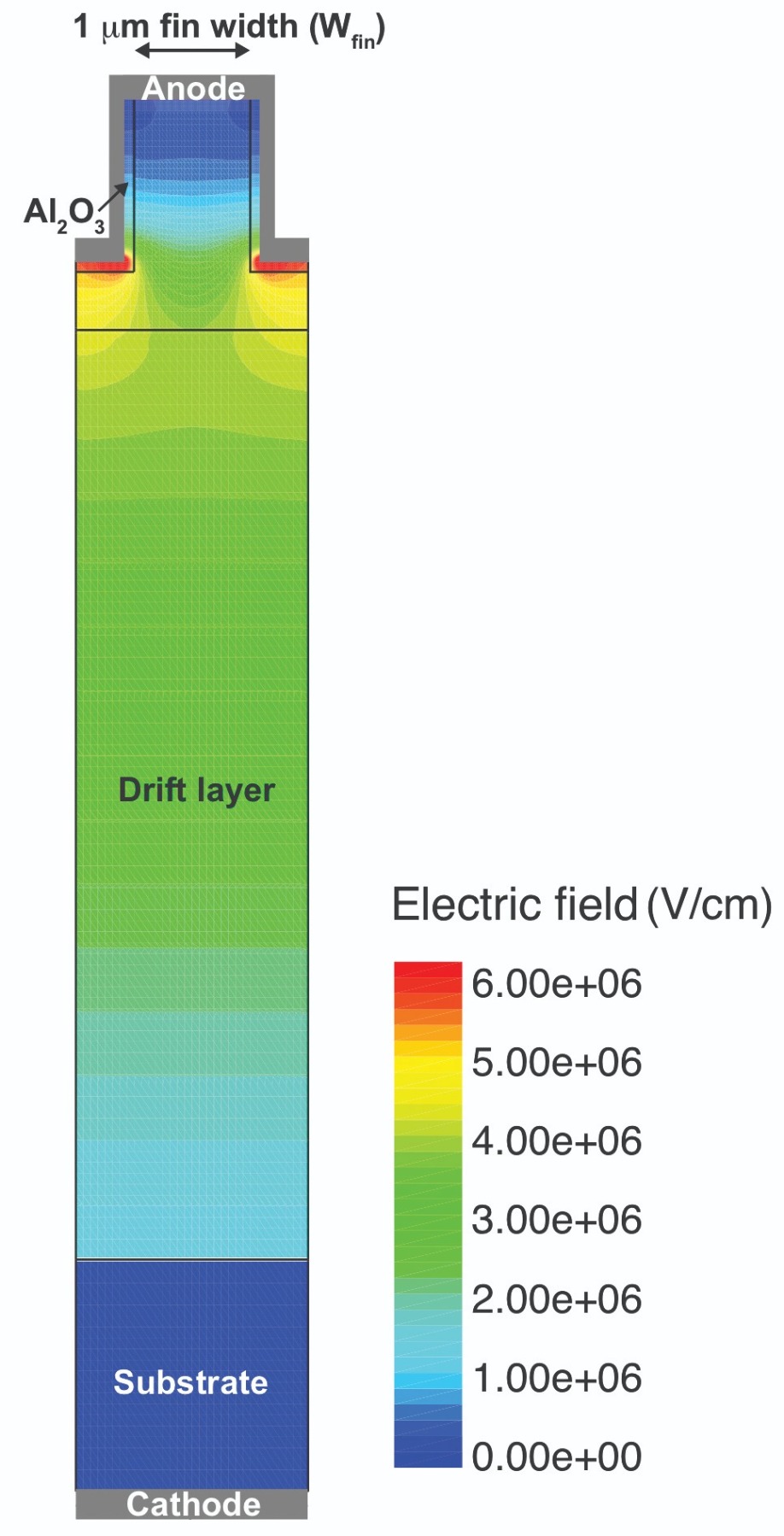
Figure 3. The simulated electric field profile in a unit cell of a trench diode with a fin channel width of 1 µm at 2.44 kV. Even though the highest parallel-plane electric field reaches 4.3 MV/cm, the electric field near the Schottky contact is less than 1 MV/cm, thanks to the charge-coupling effect provided by the trench-MIS structure. The field peaks at 5.9 MV/cm near the bottom of the trenches.
Another benefit of our architecture is that it naturally offers field-plating at the edge of the device, thereby reducing field crowding at the Ga2O3 edge structures. As the insulator must sustain a high electric field, there is a need for a dielectric material with a high breakdown field and a high dielectric constant, E. Fulfilling these requirement is Al2O3, which we add by atomic layer deposition. An additional merit of Al2O3 is its sizable bandgap, leading to a sufficiently large conduction band offset with Ga2O3 that supports suppression of the tunneling current through the MIS-junction.We produce our diodes on (001) oriented epitaxial wafers. They are produced by Novel Crystal Technology using HVPE. The drift layer, which has a net doping concentration of around 2×1016 cm-3 and a thickness of 10 µm, is designed for making devices capable of blocking 3 kV.
To investigate the influence of the fin geometry, we have produced our portfolio of diodes with fin channel widths ranging from 1 µm to 8 µm. The narrower the fin, the greater the reduction in the surface electric field, and thus the lower the expected leakage current density.
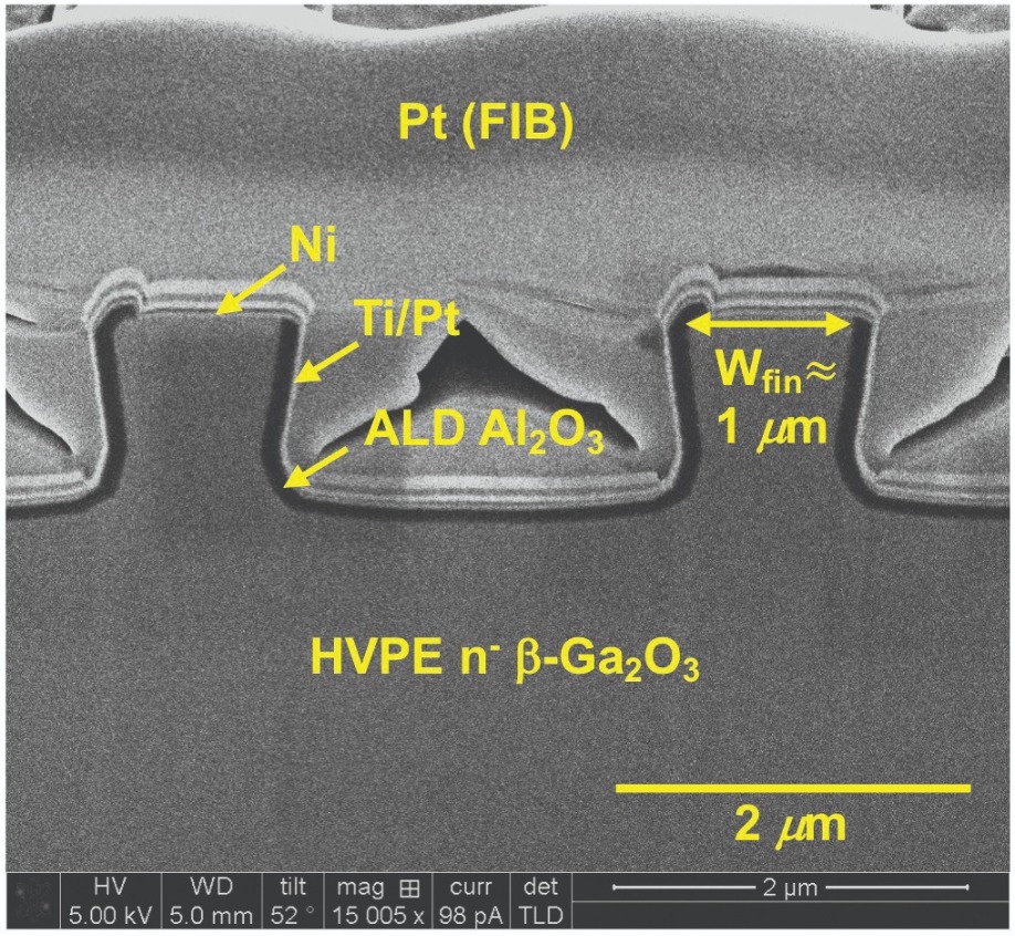
Figure 4. A scanning electron microscopy, cross-sectional image of the trench Schottky barrier diode reveals a smoothly curved trench corner profile, which is beneficial for mitigating the field crowding effect.
We form our trenches with dry-etching, using metal mask patterns. With our etching recipe, we are able to realise smoothly curved trench corners, which are seen in cross-sectional scanning electron microscopy images (see Figure 4). The smoothness of the corners helps to reduce field crowding, an issue prevalent in devices with sharp corners. After forming the ohmic contact on the backside of the wafer, we add Al2O3 with atomic layer deposition, before creating openings on top of the fin channels for the Schottky contact. This contact is formed by evaporating nickel, then sputtering titanium and platinum, to create metal coverage on the sidewall of the fin channels.Trimming leakage, boosting voltage
As expected, our trench Schottky barrier diodes turn-on at 1.25 V, a figure similar to that for a regular diode (see Figure 5). We find that the differential on-resistance of the trench diodes is governed by the ratio of the fin area to the total device area. When this figure is 50 percent, the trench Schottky barrier diode has a specific on-resistance of 10 mΩ cm2. In comparison, in a regular Schottky barrier diode this figure is just 7 mΩ cm2. The higher figure, stemming from the restricted current path within the fin channels, is the price to pay for the superior reverse blocking capability, which we will come to later on. Note that the increase in on-resistance is not fixed, and may be minimized by upping the fin area ratio and increasing the effective electron mobility in the fin channel.
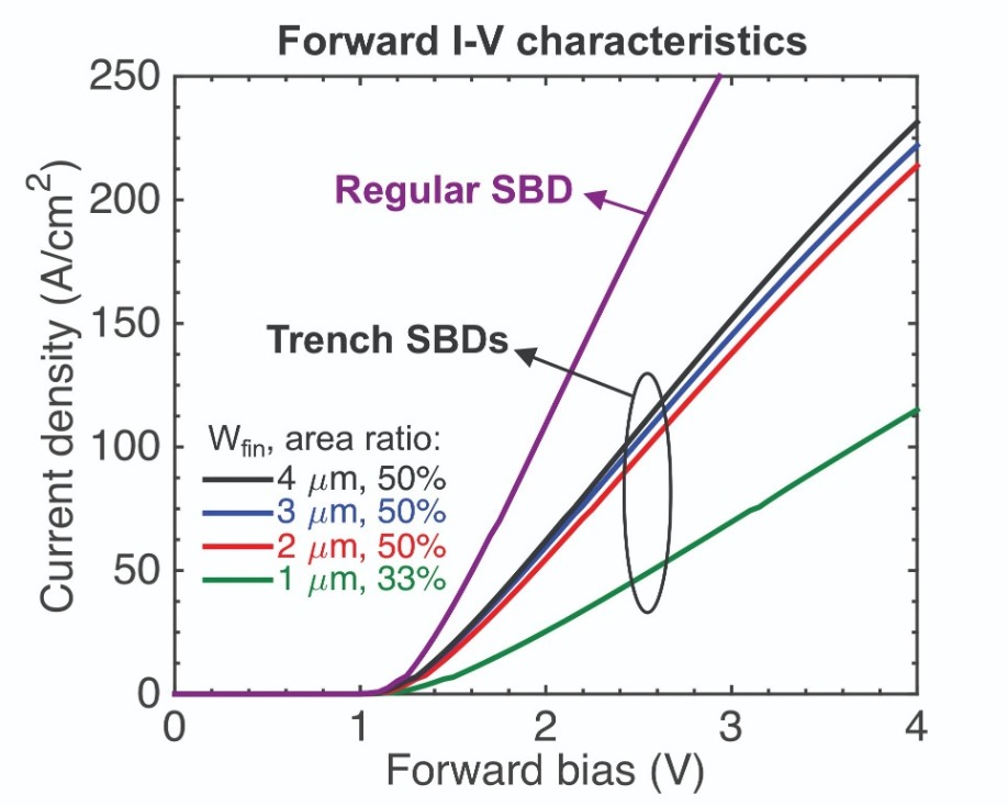
Figure 5. Forward current-voltage characteristics of the trench Schottky barrier diodes in comparison with a regular Schottky barrier diode. The turn-on voltage of all diodes is nearly identical.
The hit in the on-resistance is out-weighed by the improvement in the reverse characteristics (see Figure 6 for the reverse current-voltage characteristics of the trench diodes). We have found that compared with regular Schottky barrier diodes, our trench-based variants have a lower leakage current and a higher breakdown voltage. Our measurements also show that the narrower the fin, the lower the leakage current, due to an increase in the charge-coupling effect. Due to this, 1 µm fin channel devices have the lowest leakage current density.Our fabrication process is yet to be optimised, and there is a certain degree of non-uniformity in the leakage current. In several 1 µm and 2 µm channel devices where the parasitic leakage current is minimal, the leakage current is below our measurement noise floor of 1 µA/cm2, even at voltages exceeding 2 kV. Such a low leakage is highly beneficial, because it translates into a trimming of off-state power loss.
Even when operating at 2 kV, our low leakage devices can have a power loss on the order of mW/cm2. This is very low – to put this figure in perspective, the reverse blocking voltage in commercial kV-class Schottky-based devices is typically specified at a leakage current density of around 1 mA/cm2.
It is possible the commercial devices could sustain even higher voltages than the specified blocking voltage without destructive breakdown. However, operating in this regime would increase their leakage current and induce a high off-state power loss. In other words, the full voltage-blocking capability of the material may not be fully utilized due to the constraint imposed by the leakage current. By cutting the leakage current, we will be able to probe the intrinsic voltage handling capability of the material. Understanding the fundamental limit of Ga2O3 is essential in our push toward understanding the practicality of devices made from ultra-wide bandgap materials.
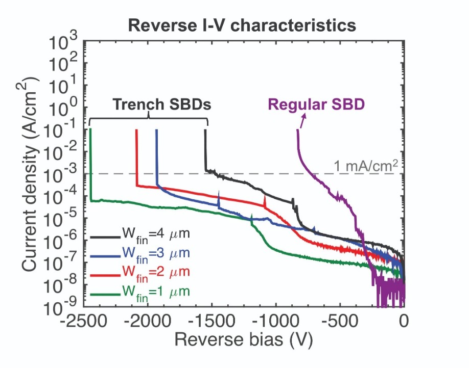
Figure 6. Reverse current-voltage characteristics of the trench Schottky barrier diodes in comparison with a regular Schottky barrier diode. The trench diodes possess a lower leakage current density as well as higher breakdown voltages.
The benefits of a narrower fin are not limited to a reduction in leakage current, but extend to an increase in breakdown voltage. This is highest in our diodes with a 1 µm channel, which have a breakdown voltage of 2.44 kV.To understand this trend, we have simulated the electric field profile at reverse bias for all our fin widths. These calculations reveal that due to field crowding, the electric field peaks at the trench bottom corners within the device’s active region. In narrower channels, the field peak is smaller, due to a reduction in space charge. Higher field peaks are best avoided, as they impair the breakdown voltage.
According to our simulations, for all widths of fin, the peak electric field in Ga2O3 hits 5.9 MV/cm at the diode’s breakdown voltage. This suggests that all our diodes, regardless of their fin width, break down at the trench corners. So, to realise high blocking voltages, smooth corners must be used alongside narrow fins. However, note that even with our latest un-optimised design, the highest parallel-plane electric field is 4.3 MV/cm, a value unreachable in SiC and GaN.
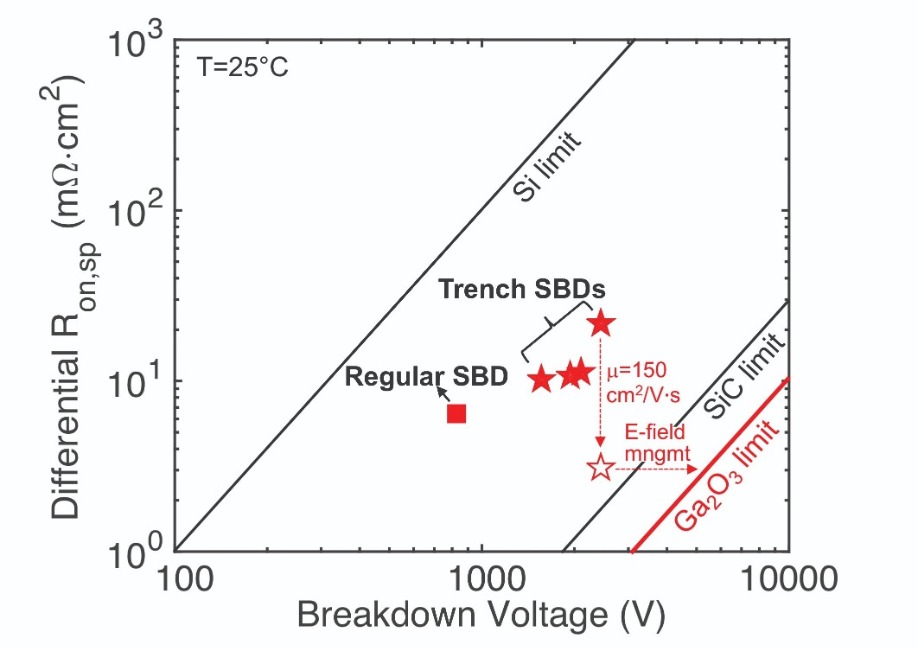
Figure 7. Trench Schottky barrier diodes fabricated at Cornell University deliver state-of-the-art performance for a vertical Ga2O3 power device. An increase in electron mobility, alongside improvements to electric field management, could spur performance to close to that of the Ga2O3 limit.
From diodes to transistorsA parallel effort of ours is the development of vertical fin channel transistors. Using a similar architecture to that of our diodes, we have fabricated the first normally-off transistor with a breakdown voltage higher than 1 kV. This result, reported last year, came from a transistor with a figure-of-merit exceeding the silicon unipolar limit.
Since then, we have increased the breakdown voltage of our normally-off transistors to more than 1.6 kV, while maintaining excellent on-resistance. As our vertical fin channel transistor shares many similarities with our trench Schottky barrier diodes, the insights that we have obtained to the device physics of these trench diodes, and also the process optimisation for this device, can be directly applied to our transistor efforts.
Marching on
At last December’s International Electron Devices Meeting (IEDM), we reported results for our trench diodes, showing that these devices set new benchmarks for breakdown voltage and the Baliga’s figure-of-merit in vertical Ga2O3 power devices. Pulsed measurements on our diodes with a 2 µm fin channel produce a Baliga’s figure-of-merit of 0.45 GW/cm2. These devices surpass the silicon unipolar limit (Figure 8), but are yet to reach the SiC limit.
Analysing the on-resistance indicates that in our latest diodes, the effective mobility is much lower than expected. We attribute this to either un-optimised surface treatments or the starting wafer quality.
If we were able to realise a mobility of 150 cm2 V-1 s-1, which has been reported in lightly-doped Ga2O3 (~1015-1016 cm-3), the on-resistance of our trench diodes would fall by a factor of three to just 3 mW cm2, leading to a projected figure-of-merit very close to the unipolar limit for SiC. Such a mobility is not pipe dream, given that the measurements for the highest room-temperature mobility in ß-Ga2O3 are around 180 cm2 V-1 s-1.
Today sales of SiC are rocketing, with GaN not far behind. This demonstrates that wide bandgap devices are starting to fulfil their promise. Next on that list will be Ga2O3, which is now making rapid progress. While the lack of native p-type doping is hampering the adoption of some conventional designs, by turning to building blocks such as MIS-junctions, we have shown that functional power devices can be made that deliver good performance. It is clear that backed up by melt-grown high-quality native substrates, Ga2O3 is able to deliver power devices with unprecedented unipolar performance and mass-production capabilities.
W. Li et al. in IEDM Tech. Digest 2018 p. 8.5.1
W. Li et al. Appl. Phys. Lett. 113 202101 (2018)
Z. Hu et al. IEEE Electron Device Lett. 39 869 (2018)


