
NREL creates cheaper GaAs solar cells
14.44 percent efficient GaAs solar cell formed on very thin layer of reformed porous germanium.
The potential to cheaply produce GaAs thin-film solar cells came a step closer to reality with the discovery of a way to reuse a surface on which the cells are made.
The findings are detailed in a paper newly published in the journal Joule, 'Germanium-on-Nothing Technology for Epitaxial Liftoff of GaAs Solar Cells' written by researchers at the US Department of Energy's (DOE's) National Renewable Energy Laboratory (NREL) and from the Republic of Korea. One of the co-authors, Jihun Oh, is a former NREL postdoctoral researcher and is now with the Korea Advanced Institute of Science and Technology.
The team's research produced a 14.44 percent-efficient GaAs solar cell formed on a very thin layer of reformed porous germanium. Improvements in the process should enable the efficiency to rise “well above 20 percent,” said David Young, a senior scientist in NREL's High Efficiency Crystalline Photovoltaics group and a co-author of the paper.
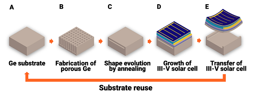
The graphic above shows how a III-V solar cell can be grown and then transferred to a new substrate.
The GON process is composed of the preparation of Ge substrate for growing III-V materials (A), formation of cylindrical pores on Ge substrate (B), pore reorganisation of Ge pores in GON structure by hydrogen annealing (C), growth of III-V solar cells on GON film (D), and transfer of thin III-V solar cells on Ge film from the Ge substrate to a foreign substrate (E).


Various types of GON structures such as sphere (F) and plate-type (G) voids can be obtained in the GON structures.
Solar cells made from elements in the third and fifth columns of the periodic table–such as gallium arsenic– have been shown to be highly efficient at converting sunlight into energy, but their high costs pose a challenge and have limited their use to niche applications, mainly in the aerospace industry. The substrate itself, which is the crystalline wafer on which the cells are grown, accounts for about 30 percent of the cost of a III-V solar cell.
But the new germanium-on-nothing (GON) approach described in the Joule paper allowed the researchers to create a thin germanium layer on top of a germanium wafer, on which a GaAs solar cell is grown. The cell and the thin layer of germanium can then be peeled off of the substrate so that the original germanium wafer can be reused.
“Silicon-on-nothing has been known for years, but this is the first time that GON has been demonstrated with a surface sufficiently smooth to allow high-quality epitaxial growth of GaAs,” said Young, whose NREL co-authors are John Simon, Kevin Schulte, and Aaron Ptak.
The process involved in the new approach creates a series of cylindrical pores in the germanium wafer. The ratio of the pores’ diameter to depth, coupled with the distance between the pores, allows for the creation of a void (nothing) between the suspended single-crystal layer of germanium and the surface of the germanium wafer. This technique could enable the cost-effective and high-volume production of single and multijunction III-V solar cells.


