
Extending the reach of photonic power
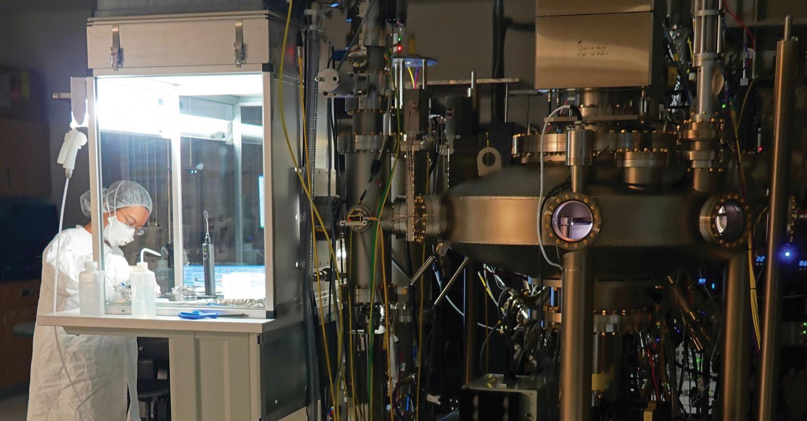
Above: Molecular beam epitaxy at the University of
Waterloo.
High-voltage photonic power converters designed for telecom wavelengths promise to extend the reach of power-over-fibre systems
BY MEGHAN BEATTIE AND KARIN HINZER FROM THE UNIVERSITY OF OTTAWA
We live in an increasingly interconnected world, depending heavily on electronic devices such as sensing and communications equipment. Delivering reliable power to these devices as they are deployed in more remote and extreme environments can be challenging. The conventional approach is to provide power over copper wire, but this is highly sensitive to electromagnetic interference and prone to heating and sparking in hazardous conditions. An alternative solution to these challenges is photonic power transmission. This involves a light source and a photonic power converter, which converts the light back into electricity.
Merits of the optical approach include full electrical isolation and immunity from electromagnetic interference. In addition, fibre is lighter and cheaper than copper cabling; it is more tolerant of the environment; and there is the potential for simultaneous power and data transmission using existing telecommunications technology.
The superiority of optical fibre for data transfer is well known in the telecommunications industry; however, there are still roadblocks to widespread implementation of photonic power transmission. In particular, long distance transmission remains a challenge – one that we are addressing in our research at the University of Ottawa with a novel chip design, operating at telecom wavelengths, that will offer tremendous improvement in the reach of power-over-fibre systems.
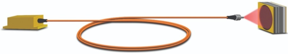
The light source for a photonic power transmission system can be either a laser or an LED. After transmission, light is transformed back into electrical power by a photonic power converter, also known as an optical power converter, photovoltaic power converter, laser power converter, or phototransducer. Optical power can be transmitted through free space, but it is usually preferable to route it through an optical fibre, which guides the light and eliminates the need for line-of-sight trajectories.
Just like solar cells, photonic power converters generate electrical power from light through the photovoltaic effect. When light impinges on the device, photons are absorbed, generating a potential difference, or photovoltage, and an electric current. However, photonic power converters have a key difference to solar cells – rather than being designed to generate as much power as possible from the very broad solar spectrum, which spans the ultraviolet to the infrared, they operate within a very narrow energy range that corresponds to the output of a laser or LED. This distinction allows photonic power converters to operate at efficiencies of up to 70 percent, much higher than a solar cell.
Photonic power has already been adopted in niche applications, powering sensors for high-voltage transmission-line monitoring and deployed in magnetic resonance imaging machines where strong magnetic fields prevent the use of copper wires.
The use of photonic power transmission is sure to grow – budding applications are numerous and varied. It is a promising option for providing power to sensors and smart electronics in autonomous vehicles, which require isolation in an electrically noisy environment. Opportunities also exist in emerging smart-grid infrastructures, which rely on vast arrays of sensors and inter-device communications, often operating in challenging environments with high voltages, electromagnetic interference and harsh weather. Other industries in which photonic power supply could make a positive impact are aerospace, avionics, defence, medicine, and telecommunications.
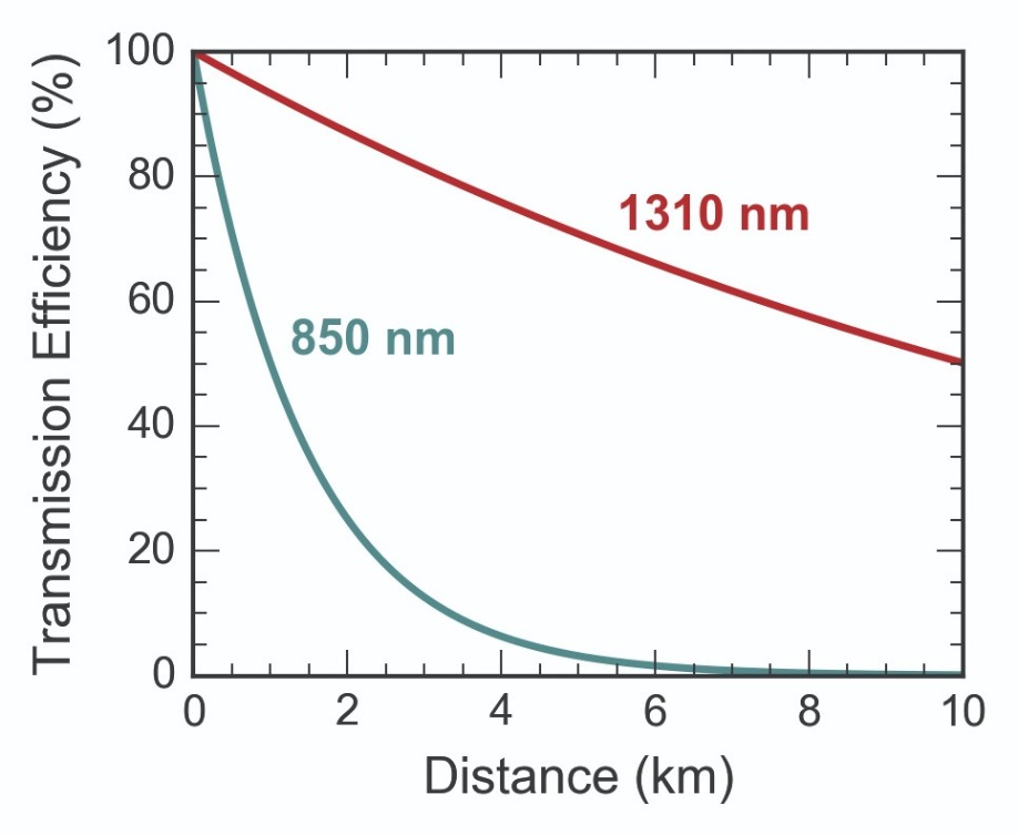
Figure 1. Optical fibre transmission efficiency as a function of distance for 850 nm and 1310 nm light. Attenuation coefficients are assumed to be 3 dB/km for 850 nm and 0.3 dB/km for 1310 nm.
Increasing the distanceAs the majority of photonic power converters are based on GaAs, their absorption lies in the 850 nm band. That’s far from ideal, because at this wavelength the optical attenuation in the fibre is around 3 dB/km – or, put another way, power halves for every kilometre it travels through the fibre. This restricts GaAs-based photonic power converters to operate in either free-space configurations, or in scenarios involving short fibre links (see Figure 1).
A far better option for power transmission over long lengths of fibre is to shift to a wavelength where attenuation is minimised. Opportunities exist in the O-band and C-band, found at 1310 nm and 1550 nm, respectively (see Figure 1 to appreciate the extent of the improvement). However, to make this adjustment, there must be a move from a GaAs-based material system to one such as InP, on which smaller bandgap absorbers can be grown.
Our team at the University of Ottawa is adopting this approach. We are developing the first vertical-segmented InP-based photonic power converters for operation at 1310 nm. To produce these devices, we are collaborating with a team at the University of Waterloo that uses MBE to make our epistructures. Grown on an InP substrate, these heterostructures feature a lattice-matched InAlGaAs absorber.
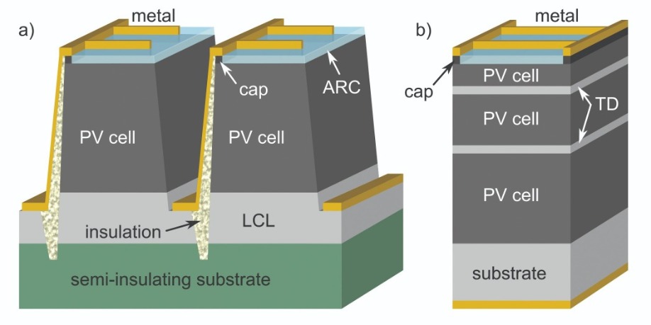
Figure 2. Typical design for a (a) lateral- and (b) vertical-segmented photonic power converter. ARC: antireflection coating, LCL: lateral conduction layer, PV: photovoltaic, TD: tunnel diode.
The move to 1310 nm slashes the attenuation in the fibre to just 0.3 dB/km, or 7 percent per kilometre, opening the door to power transfer over several kilometres. There is also the tantalising prospect of using the longer wavelength C-band for data transfer, enabling a single fibre to simultaneously provide power transfer and communication.Boosting the voltage
The operating voltage of a photonic power converter is limited by the bandgap of its light-absorbing region. GaAs-based devices, grown either by MBE or MOCVD, generate about 1.2 V, which is insufficient for most power applications. Conventional DC-to-DC converters could boost this voltage. However, a far better option for ensuring immunity to electromagnetic interference is to scale the voltage within the device itself, using series connections.
One widely used option is to form laterally segmented, interconnected devices (see Figure 2(a)) to generate output voltages of up to 20 V. This voltage is high enough to ensure that devices can be powered directly from the photonic power converter. However, this approach requires complex fabrication, and the devices that result are impaired by the strict requirement for precise alignment and uniform illumination across all segments. If one segment receives less illumination, it produces less photocurrent, limiting the current of the entire device and reducing its output power. Practical efficiencies for this type of device are typically 30 percent to 35 percent, although efficiencies under ideal conditions have hit the mid-50 percent range.
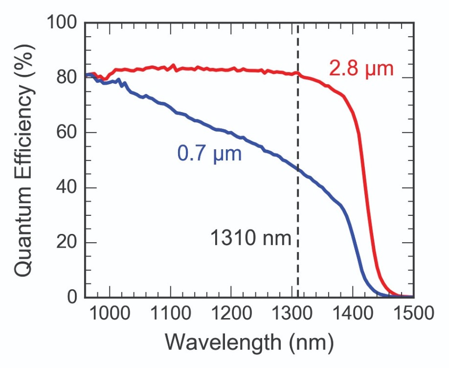
Figure 3. Quantum efficiency of optically thin, 1310 nm single-junction photonic power converters of varying thickness, designed to be incorporated into a multi-junction stack.
Due to these drawbacks, state-of-the-art photonic power converters rely on vertical interconnections, similar to multi-junction solar cell technology (see Figure 2(b)). The absorbing material is portioned into optically thin segments, series-connected with tunnel diodes. With this type of architecture, high output voltages are combined with high efficiencies. For example, a 20-junction GaAs device made by Broadcom Semiconductors ULC (formerly Azastra Opto) can produce an output voltage of 23 V. Fabrication is straightforward, and devices have good tolerance to non-uniform illumination, enabling efficiencies in excess of 60 percent. The record for efficiency, realised by Broadcom in partnership with our team, is as high as 70 percent for a five-junction device (see Table 1 for a brief overview of record efficiencies for segmented photonic power converters).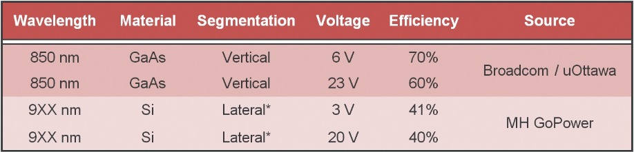
Table 1. Record segmented photonic power converter efficiencies at various wavelengths and operating voltages. *MH GoPower photonic power converters are multi-junction, but illuminated from the side so that they retain the same requirements for precise alignment and uniform illumination as standard lateral designs.
To boost the voltage of our 1310 nm photonic power converters, we employ this state-of-the-art, vertical-segmented, multi-junction design. The InAlGaAs absorbing region with a bandgap of 0.864 eV is partitioned into semi-transparent photovoltaic sub-cells. By precisely tuning the thickness of each layer, we ensure that each vertical segment generates the same current. This is accomplished with the thinnest layer at the top and the thickest at the bottom. The total thickness of the absorbing layers is almost 5 µm, ensuring at least 98 percent absorbance of incoming light. By shifting the composition of the quaternary, we can produce transparent lattice-matched tunnel diodes between each sub-cell. Ultimately, high-quality, vertical-segmented photonic power converters will be achieved.We have produced a range of single-junction photonic power converters to determine the relationship between thickness of the absorber and quantum efficiency (see Figure 3). For these test devices, we have selected layers with thicknesses that would be used in a multi-junction structure. As expected, thicker layers increase absorbance, and by extension, quantum efficiency.
One of our current activities is to establish an in-house fabrication process for device testing (see Figure 4 for a partially fabricated, single-junction photonic power converter wafer). Development of a complete multi-junction structure is also underway.
To benchmark the performance of our devices, we use the detailed balance limit. This represents the theoretical limiting efficiency of the device, and assumes that every absorbed photon generates a single electron-hole pair, completely separated and perfectly conducted. Calculations are carried out in the radiative limit, so excited charges can only relax by radiating light that may be reabsorbed in the device. These calculations offer an upper limit on what can be realised, as real devices are impaired by imperfect absorption and conduction, as well as non-radiative forms of charge relaxation. As we improve material quality, the performance of our devices gets closer to the limiting efficiency.
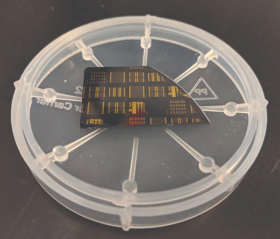
Figure 4. Single-junction photonic power converter chips for O-band operation.
For our design, the theoretical voltage per junction is 0.63 V, in the radiative limit for an input power density of 10 W cm-2. Based on these results, an ideal 10-junction photonic power converter of our design could achieve an output voltage over 6 V, and a limiting efficiency of 65 percent. For realistic material, a 10-junction photonic power converter should power a 5 V device with an efficiency of between 50 percent and 60 percent. Cranking up the input power, the current will increase linearly and voltage logarithmically. These changes would push the limiting efficiency to over 70 percent in the radiative limit for 100 W cm-2.Further improvements in the voltage and the efficiency will result from moving to a slightly larger bandgap for the absorbing region, aligning the absorption edge to the incoming light at 1310 nm – which corresponds to a photon energy of 0.95 eV – and thereby reducing the amount of energy lost to heat. Note that maintaining absorbance at 98 percent requires the use of a thicker absorber.
Possibilities and challenges
With our design of photonic power converter, we expect to transmit 1310 nm photonic power over a 1 km length of optical fibre with a 56 percent efficiency. That’s nearly a two-fold increase over a comparable GaAs-based 850 nm system. The performance provided by our 1310 nm link paves the way to powering 5G devices within the internet-of-things. Even for distances as long as 10 km, we expect 30 percent efficiency, a tremendous improvement over GaAs-based devices, which can only realise a 0.06 percent efficiency (see Table 2 for a summary of estimated efficiencies).
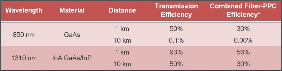
Table 2. Estimated efficiencies for power-over-fibre systems assuming 60 percent photonic power converter efficiency. *Does not account for efficiency of the light source (laser or LED).
Within a full power-over-fiber system, the overall electrical-optical-electrical efficiency is not just determined by the efficiency of the photonic power converter and the extent of fibre attenuation, but also by the efficiency of the light source. For high-power lasers operating at 1310 nm, efficiencies can reach the mid-30 percent range. Assume an electrical-optical conversion efficiency of 35 percent, and a photonic power converter efficiency of 60 percent, and the electrical-optical-electrical efficiency can be as high as 21 percent through free space. Add in 1 km and 10 km lengths of fibre, and the total efficiency will drop to 20 percent and 11 percent, respectively, assuming perfect optical coupling.These efficiencies indicate that fully optical power-over-fibre systems could be deployed over distances up to 10 km, delivering reasonable performance and enabling reliable, fully isolated power supply to hazardous environments. Crucially, this power transfer technology could be added to existing fibre networks, previously reserved for data transfer, by introducing a 1310 nm light source and a photonic power converter.
Our efforts, and those of our peers, are expanding the versatility of power-over-fibre systems. As the reach of photonic power extends, the catalogue of applications will continue to grow. There is no doubt that this technology has a very bright future.
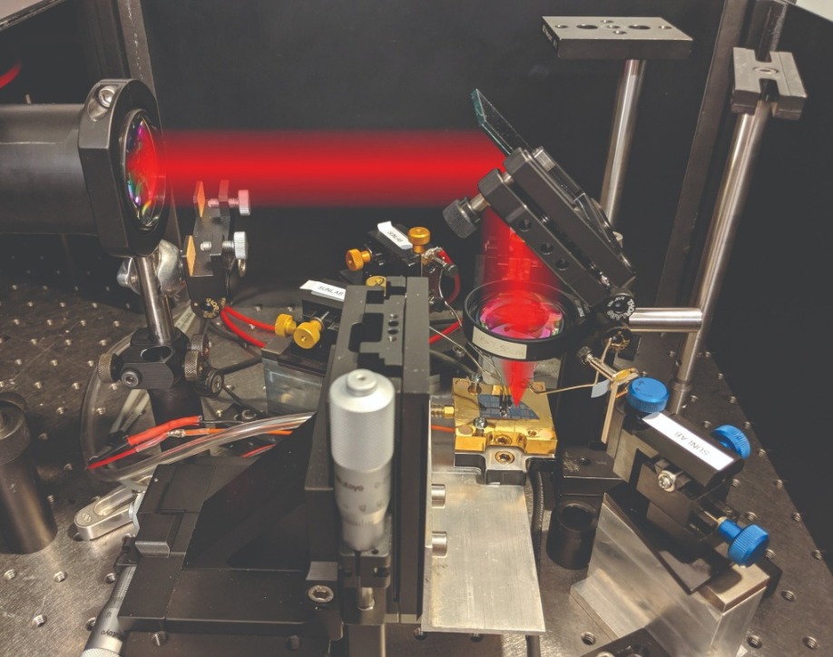
Experimental setup to measure current-voltage characteristics for photonic power converters with overlay of beam path.
D. Xia et al. “Opportunities for High Efficiency Monochromatic Photovoltaic Power Conversion at 1310 nm,” 46th IEEE PVSC, June 2019
M. Wilkins et al. IEEE Trans. Power Electron. 34 1054 (2019)
S. Fafard et al. Appl. Phys. Lett. 108 071101 (2016)


