
Optimising GaN heterostructures for 5G

Combining AlN or InAlN barriers with SiN passivation layers leads to exceptional performance for GaN RF devices, regardless of the choice of substrate.
By Markus Behet, Joff Derluyn, Stefan Degroote and Marianne Germain from EpiGaN/SoiteC
The roll-out of 5G is great news for GaN. It is predicted to propel the market for RF devices made from this wide bandgap semiconductor to more than $2 billion by 2024, according to the French market analyst Yole Développement.
The move from 4G to 5G should be seen as part evolution, part revolution. Grabbing the most attention is the availability of enhanced mobile services, resulting from faster speeds, ultra-low latency, and a reduction in power consumption. However, 5G will also bring further investment in traditional machine-to-machine and internet-of-things applications, and open up new market opportunities in mission critical services, such as autonomous vehicles, drones and ‘telehealth’. It is even expected that 5G will act as a catalyst for transformative changes of work processes, and will establish a new set of rules for competitive economic advantages. So great are these changes that IHS Markit forecasts 5G to enable $13.2 trillion of global economic output in 2035.
As 5G networks are rolled out, there will be far greater densification at the macro scale. More base stations will appear, featuring devices operating at far higher power densities. But that’s not the only change. To alleviate the load on macro cells, there will also be an emergence of smaller network cells – known as pico and femto cells – to increase network capacity and provide extended coverage.
5G deployment is also changing the frequencies of the RF signals, and the way they are transmitted and received. It is designed not only for spectral bands below 3 GHz, where most mobile communications happen today. It also utilises mid bands between 3 GHz to 6 GHz – a spectral domain known as sub-6 GHz – and new frequency bands previously thought unsuitable for mobile communications, such as high bands in the millimetre-wave region, above 24 GHz. In both these domains, bandwidths exceed 100 MHz. A further increase in throughput and data rates comes from a switch from a standard antenna architecture to one that is based on the multiple input and the multiple output of many signals – this is referred to as massive MIMO. And yet another advancement is active antenna beam steering at the base station, to maximise spectral efficiency.
Increased deployment of small cell antennas during the roll-out of 5G will drive demand for compact, highly efficient RF devices. Designers of massive MIMO systems may find it even more challenging to manage power consumption and heat dissipation than the complexity of antenna arrays. In 4G systems, there has been a priority on the power consumption of the power amplifier when designing base station heat sinks and power supplies. But now concerns are shifting, because power consumption of the signal processing electronics in 5G massive MIMO systems is approaching that of the power amplifiers. This means that semiconductor efficiency will become key.
For both 5G infrastructure and handset architectures, mandatory attributes for RF semiconductor devices are efficiency, compactness, low cost, high power density and linearity. Judged in terms of wideband performance, power density and efficiency, legacy technologies – essentially silicon LDMOS or GaAs – are no match for GaN HEMTs, regardless of whether they are grown on silicon or SiC. It is this technology that is meeting stringent thermal specifications for 5G, while preserving valuable PCB space for the tightly clustered mMIMO antenna arrays. In base stations, discrete designs are already being replaced by space-saving multi-function GaN MMICs and multi-chip modules.
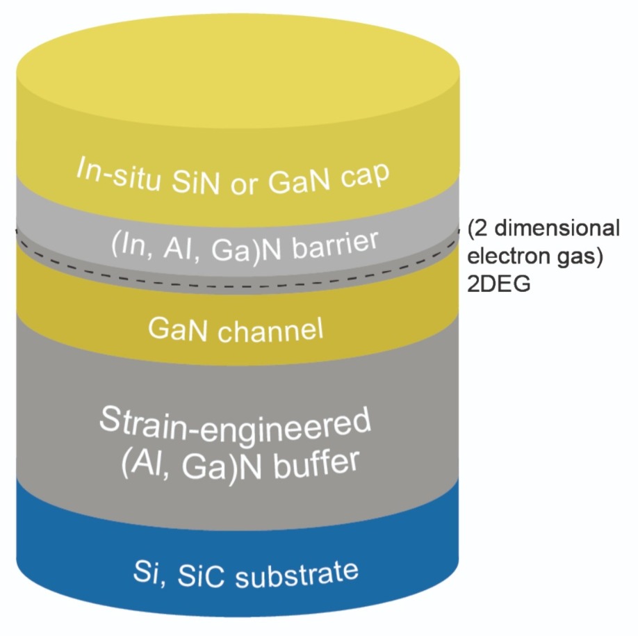
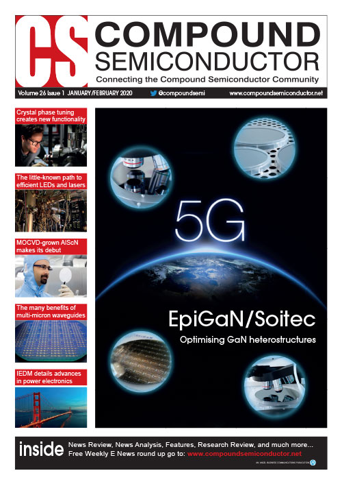
Figure 1. A typical GaN HEMT heterostructure.
Two flavours of GaNWhen producing GaN HEMTs, an important decision is the choice of substrate. Semi-insulating SiC is selected to meet the need for ultimate power levels in the most demanding applications, while silicon’s strengths are related to low-costs, large diameters and high-volumes.
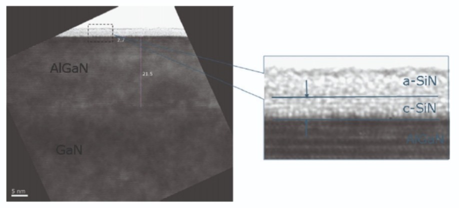
Figure 2. Transmission electron microscopy of an in-situ SiN-capped AlGaN/GaN HEMT structure showing the nature of the SiN. This material is crystalline close to the interface to the barrier, and amorphous when further from it.
However, it would be wrong to think that it is only the choice of substrate that determines the bang-per-buck. This can also be governed by the choice of the barrier layer, the quality of the passivation, and characteristics such as the uniformity of the wafer.At epiwafer supplier EpiGaN, now part of Soitec, we leave it to our customers to decide whether a SiC substrate, or one made from silicon, is the best choice for their RF application. Our focus is to produce the best GaN HEMT heterostructure for a specific application on each of these foundations, through judicious choice of the barrier and the cap layer.
In order for GaN-on-silicon to compete directly with GaN-on-SiC in high-end RF applications, a few technical hurdles have to be overcome. Some of these are intrinsic, including the lower thermal conductivity of silicon compared with SiC – in this case, the solution is an aggressive reduction of the substrate thickness to 50 µm. But there are also other issues, such as the conductive interface that is formed between the silicon substrate and the III-nitride buffer layer during epitaxial deposition. This parasitic conduction path is highly detrimental, as it capacitatively couples to the HEMT channel. It is to blame for the undesired dissipation of RF signals, which increase with frequency. When transistors are manufactured on such lossy substrate/buffer combinations, they fail to deliver good performance at high frequencies, in terms of gain, power and efficiency.
To suppress this undesirable conductive path, we have developed and optimised a robust interface technology. This trims RF signal loss on GaN-on-silicon material to well below 0.4 dB/mm for frequencies up to Ka-band. Such a low loss enables the RF performance of GaN-on-silicon HEMTs to get very close to that of their GaN-on-SiC cousins. Using this process, which can be used on high-resistive silicon substrates up to 200 mm diameter, we have produced epiwafers that are ideal for making devices for the 5G sub-6 GHz and millimetre-wave frequency bands.
Figure 3. 110 nm gate length GaN-on-SiC HEMT structure using a 3 nm AlN barrier capped with 10 nm in-situ SiN; courtesy of F. Medjdoub, IEMN, Lille.
One barrier fits all? Not at all!Today, the workhorse for RF power amplifiers operating in sub-6 GHz bands is a GaN-on-SiC HEMT with a 20 nm-thick AlGaN barrier that has an aluminium content of around 25 percent. This ternary barrier is capped and protected by an ultra-thin GaN layer, typically 2-3 nm thick (see Figure 1).
Our view is that there are times when this mainstream barrier may not be the best choice in more demanding millimetre-wave band and low-voltage applications. For these cases, we have developed heterostructures that combine an in-situ SiN protecting layer with either a binary AlN layer or a lattice-matched InAlN barrier. We will now outline the merits of both these options for the barrier.
One of the strengths of the binary AlN barrier it that it allows a reduction in the thickness of this layer from typical values of around 20 nm to between just 3 nm and 6 nm. This opens the door to bringing the transistor gate very close to the densely populated channel, and in turn maximising the electrostatic coupling between the two – this leads to improved gate control, and ultimately superior RF transistor characteristics.
For example, the transistor’s transconductance increases when the gate is brought closer to the channel. In addition, there is a suppression of short channel parasitic effects, which can impair transconductance when scaling transistor gates below 0.15 µm. Another benefit of the AlN barrier is that it has a very high inherent piezoelectric effect, resulting in carrier densities in excess of 2 x 1013 cm-2 in the transistor’s two-dimensional electron gas. This leads to a hike in power density, and also a significant reduction in chip size, so long as an appropriate thermal chip layout is used.
By turning to InAlN, rather than AlN, it is possible to produce a lattice-matched barrier by using the alloy In0.17Al0.83N. Pairing this ternary with GaN is attracting much attention, because this combination has a large spontaneous polarization, but is not impaired by a high degree of strain, which is found in AlGaN/GaN. These merits enable heterostructures of InAlN/GaN to have significantly higher sheet carrier densities than those of AlGaN/GaN, while maintaining good electron mobility. At the device level, this means that HEMTs have higher maximum current capabilities, a valuable asset for high-power devices operating up to millimetre-wave frequencies.
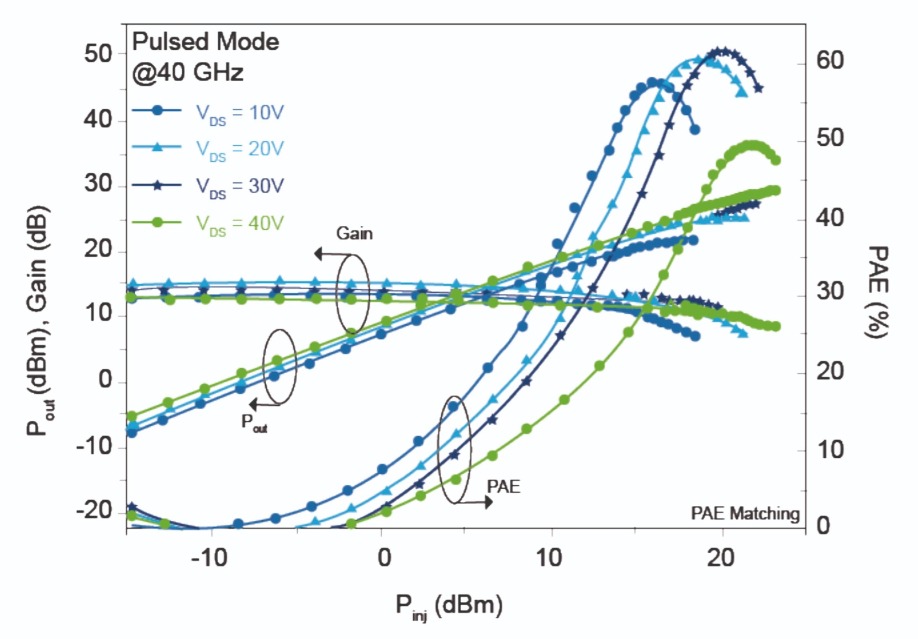
Figure 4. Pulsed power performance at 40 GHz of a 2 x 50 µm AlN/SiN HEMT (gate length 110 nm, gate-to-drain spacing of 1.5 µm) at Vds of 10 V, 20 V, 30 V and 40 V*, *power matching only; courtesy of F. Medjdoub, IEMN, Lille.
We have developed InAlN/GaN heterostructures on both SiC and silicon substrates. Using lattice-matching conditions, and InAlN barrier thicknesses of 10 nm or less, we can produce material with a typical sheet resistivity around 220 Ω/sq, a mobility of 1700 cm2 V-1 s-1, and a sheet carrier density of 1.6 x 1013 cm-2.On the top of our epiwafers we add a high-quality SiN layer, grown in-situ by MOCVD. As the first few monolayers of the SiN are crystalline, the interface trap density is very low (see Figure 2).
This SiN layer can serve many purposes. It can provide surface passivation, sealing the top of the GaN wafers directly after growth; it can be used as a gate dielectric; it can stop relaxation of the strained barrier layers; and it can prevent exposure of III-N layers to the fab environment, enabling the processing of GaN-on-silicon wafers in silicon CMOS fabs.
Yet another benefit of the in-situ SiN capping layer is that it controls the filling of the surface states during device operation. This can combat current collapse, which is associated with the depletion of the two-dimensional electron gas. Current collapse is avoided because the addition of SiN provides enough charge to neutralize the surface charge of the AlGaN barrier layer, so that its surface potential no longer contributes to the two-dimensional electron gas depletion. Finally, when SiN layers are added to HEMTs, these devices have a superior stability at high temperatures.
Millimetre-wave merits
For devices operating in the 5G millimetre-wave bands, a premium is placed on performance at high frequencies. HEMTs are scrutinised for their gain, power density and power-added efficiency, and this reveals that those that are made from standard AlGaN/GaN heterostructures are not the best choice for Ka-band 5G massive MIMO antenna systems. A better option for these challenging specifications are designs that feature ultra-thin AlN or lattice-matched InAlN barriers in combination with in-situ SiN cap layers. HEMTs with these hallmarks deliver excellent performance, by suppressing short-channel effects while simultaneously realising the highest current densities.
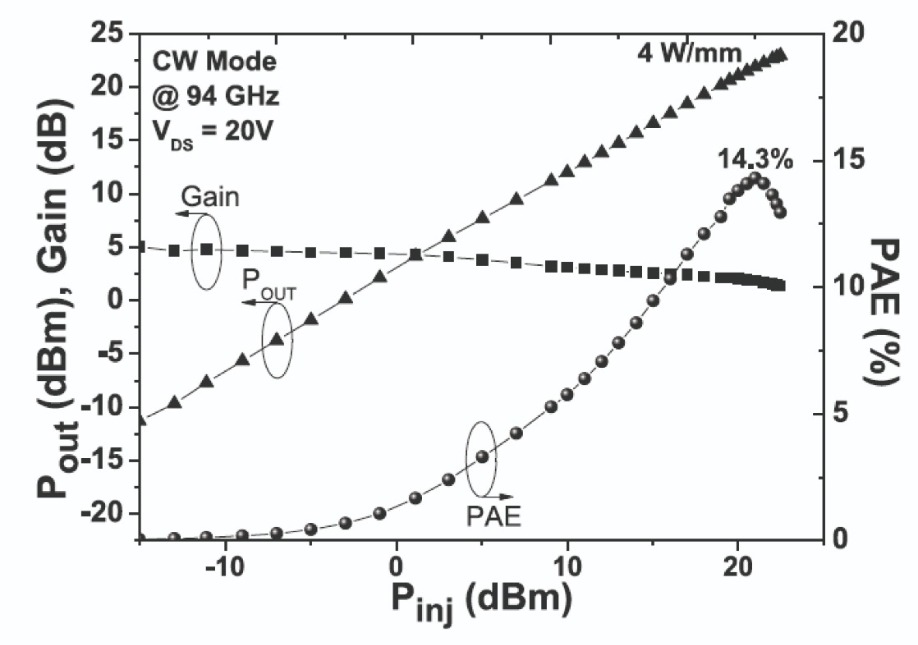
Figure 5. Continuous-wave power performance at 94 GHz of a 2 x 25 µm AlN/SiN HEMT (gate length 110 nm, gate-to-drain spacing of 0.5 µm) at Vds=20V; courtesy of F. Medjdoub, IEMN, Lille.
To produce exceptional high-frequency performance, it is necessary to scale-down the device dimensions while using an optimized heterostructure to mitigate short-channel effects under high electric fields. Working in partnership with engineers at IEMN-CNRS, we have done just that. The small transistors that have been produced, which feature a 3 nm-thick AlN barrier capped with a 10 nm-thick in-situ layer of SiN (see Figure 3), produce a state-of-art power-added-efficiency. Driven in pulsed mode, this efficiency is around 60 percent at 40 GHz, for drain-source voltages up to 30 V (see Figure 4). The output power density saturates at 5.4 W/mm. When this voltage is increased to 40 V, power-added-efficiency still exceeds 50 percent, for a saturated power density of 8.3 W/mm. This excellent level of performance is maintained even at much higher frequencies – at 94 GHz, in-situ SiN capped AlN/GaN transistors with a gate length of 110 nm produced an outstanding 4 W/mm at drain-source voltage of 20 V (see Figure 5). Preliminary large-signal robustness assessments also produce promising results. During operation for 24 hours, there is no sign of device degradation, thanks to superior in-situ SiN surface passivation that enhances surface robustness.We have also collaborated with Ommic, a leading 150 mm European GaN foundry, to provide further proof of the performance of devices produced with our material. Ommic has developed a 100 nm gate-length, open foundry MMIC process with a complete design kit on our SiN/AlN/GaN-on-silicon HEMT technology.
The devices produced in the Ommic line provide further verification of the superiority of GaN HEMTs made with our material over standard GaAs pHEMT processes. The breakdown voltage is much higher, hitting 40 V, and this leads to a much higher Ka-band output power density – it is 3.5 W/mm at 30 GHz – alongside a higher robustness to input mismatch conditions.
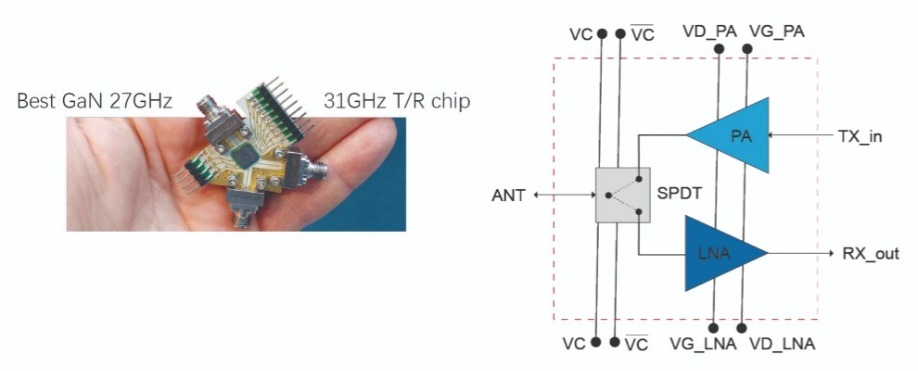
Figure 6. Fully integrated millimetre-wave 5G 26-34 GHz transmitter/receiver product utilising EpiGaN’s GaN-on-silicon RF HEMT epiwafer technology; courtesy of Ommic, Limeil Brévannes, France.
Designers at Ommic have also produced a fully integrated 5G 30 GHz transceiver (see Figure 6) and a 5G 40 GHz power amplifier. The chip size of the 30 GHz, GaN-on-silicon transceiver is only 11 mm2. Output power from the amplifier and switch transceiver part exceeds 35.5 dBm, while the gain of the low-noise amplifier and switch transceiver part in receive mode is above 20 dB, an excellent value (see Figure 7). Meanwhile, a 40 GHz GaN-on-silicon power amplifier has characteristics that include a P1dB of 10 W, a linear gain of 20 dB and power-added efficiency above 20 percent when operated at 9 dB backoff (see Figure 8).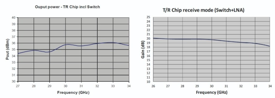
Figure 7. Transmitter power amplifier output power and receiver small-signal gain of a millimetre-wave 5G GaN-on-silicon transceiver MMIC shown in Figure 6; courtesy of Ommic, Limeil Brévannes, France.
Our collaborations with IEMN-CNRS and Ommic highlight the tremendous capability of RF GaN technology for 5G cellular networks. Whether designers select GaN-on-SiC, or would be better off with GaN-on-silicon, depends on specific requirements such as the cost versus performance trade-off for a particular RF application. GaN-on-SiC is already grabbing market share from silicon LDMOS technology in 4G-LTE base station radio heads, and enjoying success against GaAs pHEMT technology in millimetre-wave, point-to-point backhaul systems.At the same time, GaN-on-silicon is quickly closing the performance gap, while offering an attractive opportunity to drive down costs through economies of scale. This is helping RF GaN technology to start to enable innovations in many existing applications.
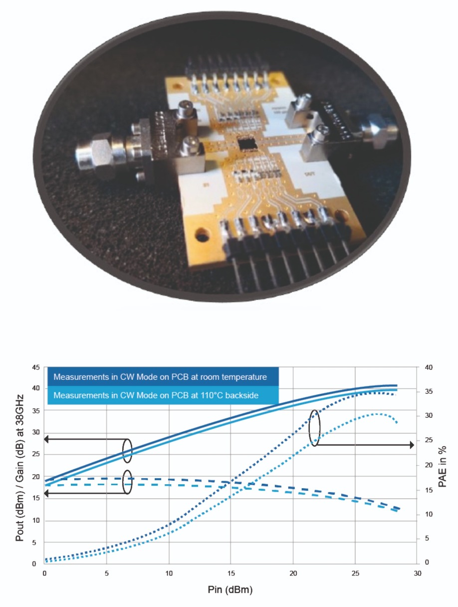
Figure 8: Output power, gain and power-added efficiency of a 5G 40 GHz GaN-on-silicon power amplifier; courtesy of Ommic, Limeil Brévannes, France.
With any semiconductor technology, true mass-market adoption requires a mature supply chain. This is starting to take shape with RF GaN technology for 5G. We see independent device manufacturers and pure-play foundries positioning themselves to build up a solid supply chain for RF GaN device manufacturing.What about the smartphone, now the holy grail for every semiconductor technology? At first glance GaN is not ideal, as the higher supply voltages – typically 10 V or more – are not well suited to handsets, which typically use between 3 V and 5 V. But that’s not a show-stopper as this gap can be bridged with device process adaptations. Some of the biggest component suppliers in the handset business are already discussing GaN-on-silicon for 5G millimetre-wave enabled smartphones.
Standards will continue to evolve, due to the introduction of carrier aggregation and the ever increasing performance requirements for multi-mode, multi-band power amplifiers. This may play into the hands of RF GaN-on-silicon technology, which offers the inherent benefits of scaling, and could soon become a strong contender for 5G mobile devices.


