The benefits of multi-micron waveguides

Increasing the size of the waveguide on a photonic integrated circuit significantly reduces optical loss, boosts power handling and enables efficient coupling to the laser.
BY AARON ZILKIE AND GREG FINN FROM ROCKLEY PHOTONICS
Silicon photonics holds the key to bringing photonic integrated circuits (PICs) to many more applications. PICs that sport silicon photonics promise to: increase the bandwidth and the power efficiency in data centres; provide low-cost, solid-state technologies for LiDAR operating at eye-safe wavelengths; deliver advanced computing solutions; and transform network communications, sensing and 3D imaging.
Today, the majority of silicon photonics players are focusing their efforts on developing monolithic products, which integrate photonics structures with CMOS on a single semiconductor chip. At first glance this is an attractive approach. However, if you delve more deeply drawbacks appear. One of the biggest of these is that due to physical and economic considerations, CMOS silicon photonics is not going to fulfil its full potential and scale. Why? While the scaling of CMOS technologies delivers benefits to the performance of electrical circuits, success is not replicated with photonics. Instead, multiple issues arise, because key photonics structures struggle at sub-micron dimensions. There is also another major issue – the materials available within a traditional CMOS semiconductor process cannot support the implementation of every electro-optic structure. Take, for example, the laser, which requires the processing of III-V materials.
The technology that we have developed at Rockley Photonics takes into account all these issues. Our approach is to begin with a clean sheet – a completely different process flow, unconstrained by the limitations of legacy CMOS processes that have been optimised for VLSI electronic devices.
From this starting point, we have been developing and optimising a proprietary photonics manufacturing technology since our foundation in 2013. We are able to draw on a depth of expertise that goes back some thirty years, and is aided by our close working relationship with our foundry partners. The platform that we are pioneering has great versatility, offers broad applicability across many product applications and markets, and enables high-volume production.

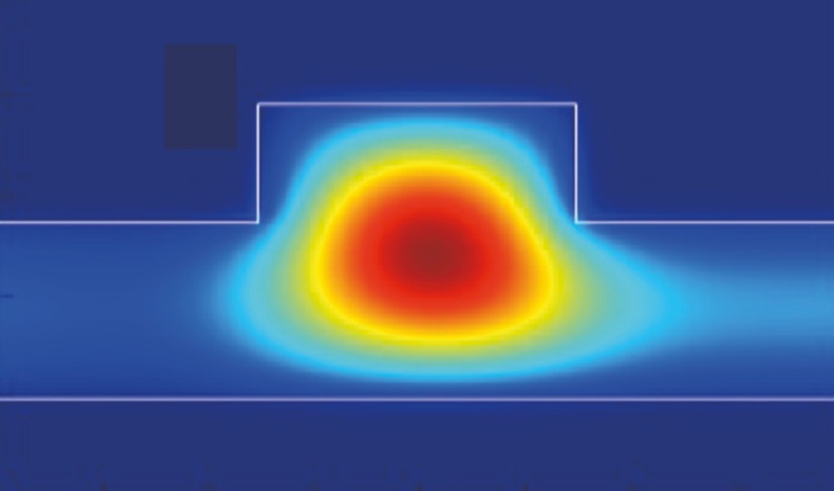
Simulation shows excellent confinement for single-mode light propagation in Rockley Photonics’ 3 µm-high waveguides. This single-mode propagation is maintained even if the waveguide is excited off-centre.
Bigger is betterAt the heart of our technology is the use of larger, multi-micron waveguides, which hold the key to optimising PIC performance, power efficiency, manufacturability and versatility. Compared to a conventional architecture, our platform has: up to ten times lower waveguide loss; a 25-fold reduction in performance variability, due to changes in waveguide dimensions; polarization independence; and a low-loss, monolithic, ultra-broadband fibre attach technology.
By reducing propagation loss, our multi-micron waveguides enable PICs to serve the widest possible range of applications. We tackle the leading contributor to propagation losses, electromagnetic field scattering, which is caused by roughness in the sidewalls of the waveguide. Reducing this roughness is far from easy – a simpler approach is to minimise the transmitted light’s modal overlap with the side walls. This is what we do with our multi-micron waveguides, to make them outperform their conventional sub-micron equivalents. Our waveguides combine improved confinement with a reduction in modal overlap with waveguide side walls – factors that also enable high integration capabilities.
In many applications, it is important for a PIC to have a high power-handling capacity. For example, with LiDAR, high output powers enable the generation of images at extended ranges and high frame rates – leading to the delivery of more photons on target down range. With silicon photonic chips, power-handling capacity is limited by a saturation effect associated with the simultaneous absorption of two photons. This absorption loss is governed by the spatial intensity of the light in the waveguide, so is substantially different in sub-micron and multi-micron waveguides. In 3 µm waveguides, power can be 30 times higher than it is in 220 nm waveguides before there is a 1 dB power loss due to two-photon absorption.
Another valuable attribute for 3 µm waveguides is that they support single-mode operation, which minimises dispersion and signal degradation. It may come as a surprise to some that our multi-micron waveguides are capable of this – and they do so while offering several advantages over a conventional sub-micron variant, including simultaneous realisation of low-loss coupling to standard single-mode fibre and III-V active devices, very low propagation losses, high tolerance to fabrication variations and polarization independence. The latter is realised by setting the waveguide rib width-to-height ratio close to unity, and ensuring that the transverse electric and transverse magnetic modes have similar values for the effective index. We produce PICs that have all these attributes and a range of waveguide sizes with cross-sectional dimensions from 1 µm to 13 µm.
An additional merit of multi-micron waveguides is that they can realise tight bends. This is highly valued – designers want to produce high-density photonic circuits, so they are keen to avoid large bends that hinder compact PIC designs, waste valuable silicon space and result in larger chip and package sizes. Our multi-micron waveguides are ideal, as they can have tight bends while avoiding losses and mode leakage, because they provide strong confinement of the electromagnetic wave. To do this, we convert the rib waveguides into strip or wire waveguides in the parts of the circuit where tight bends are needed, and employ a special design known as an Euler bend in the high-confining strip waveguide.

Bends in Rockley’s 3 µm waveguides.
It is essential to have precise phase control in circuits, to ensure excellence in filtering, switching and beam steering, and to fix the laser wavelength. Phase is influenced by the properties of the waveguide, such as its refractive index and its dimensions, including its length. If the waveguide has a non-uniform profile across a wafer, its characteristics will vary, leading to errors in phase and variations in the filter centre wavelengths.We have shown through simulation and measurement that our multi-micron waveguides produce a far lower phase error and wavelength variation than sub-micron counterparts. For a 3 µm waveguide, the variation in effective refractive index is 20 to 40 times lower than it is in 220 nm waveguides.

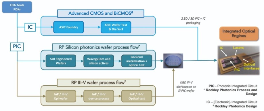
Rockley Photonics manufacturing flow.
Building blocksIn addition to developing multi-micron waveguides, we have created a portfolio of key building blocks. They include lasers, modulators, photodetectors and filters, all of which utilise the attributes of the platform.
To add a laser to our PIC, we have to integrate a III-V semiconductor device, because silicon is a poor light emitter. This addition is relatively easy for us, because laser diodes naturally also have a multi-micron mode size.
We attach the fully processed lasers directly, in a recess that we etch into the silicon waveguide. This facilitates edge coupling, which enables low-loss and dense laser integration to produce PICs with a compact form factor, while still realising high manufacturing tolerances. This approach is also highly versatile, enabling us to integrate a wide range of lasers – different materials and designs – using a flip-chip die bonding approach.
The lasers that we add have excellent characteristics. They have very narrow linewidths and output powers that can exceed 50 mW at room temperature. Those with a hybrid distributed feedback design are tolerant to back-reflections, having up to -20 dB return loss at the laser facet. This is a very valuable attribute, as commercial lasers used in silicon photonics have to operate in the presence of multiple sources of scattering and back reflection.
Our platform is also ideal for ultra-broadband applications. It can produce many-channel laser PICs, built by harnessing multi-cavity and multi-material wafer-scale integration techniques.
We have also developed processes for adding electro-absorption modulators and photodetectors to our chips. These devices are critical components in products across multiple markets including optical fibre and datacentre communication transceivers.

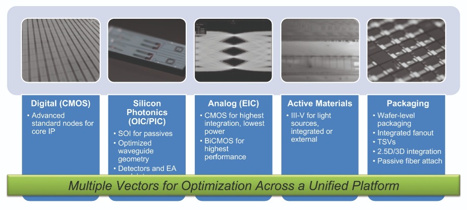
A well-diversified toolbox enables platform versatility.
Through variations in voltage, modulators adjust the intensity of the output of the laser, encoding it with a high-speed signal. Combining these devices with sub-micron silicon waveguides requires costly, specialised processing techniques, and wastes large volumes of expensive III-V material. In sharp contrast, thanks to our multi-micron platform, we can employ standard, efficient III-V foundry processes. The modulators that result deliver excellent performance with state-of-the-art 50 Gbit/s NRZ and 100 Gbit/s PAM-4 signals.Germanium photodetectors, which convert light signals back to electric signals, are also made in this platform with excellent performance. These polarization-independent, broadband devices have electro-optic detection bandwidths of over 40 GHz, sufficient for detection of 50 Gbit/s NRZ and 100 Gbit/s PAM-4 signals.
Filters are an essential ingredient in PICs, performing functions that include wavelength-division multiplexing, a technology that enables high-bandwidth data transfer. The most common way to realise this is to use arrayed waveguide gratings. This form of filter is far better with multi-micron waveguides than sub-micron variants, because the larger dimensions lead to a lower birefringence, polarization independence, and a reduction in phase errors and propagation losses. Thanks to these attributes, arrayed waveguide gratings, produced in our platform, provide high performance and repeatability. By incorporating Euler bends into these arrayed waveguide gratings, they are far more compact, opening the door to their integration into high-density PICs.
One of the downsides of forming PICs with silicon is that this material has a high thermo-optic coefficient, which hampers heat management. To address this, we deploy heaters that deliver around a 1 mW/p phase change – they can be positioned within waveguides to manage thermal energy. In addition, with just a few additional processing steps, our arrayed waveguide gratings made with only silicon can be made temperature independent. These gratings produce almost no drift in wavelength due to temperature variation.
For many applications, optical signals need to be transferred from the chip to the fibre. This requires an interface between PIC waveguides and single-mode optical fibre. If the PICs are to be competitive in high-volume products, this attachment should be low-cost, low-loss and simple to align.
We tick all those boxes, thanks to the use of a mode size that is in the same ballpark as that of single-mode fibre. A single-stage spot size converter enables us to mode-match between 3 µm waveguides and 13 µm waveguides, and then directly couple to single-mode fibre. Etching V-grooves into the silicon allows us to accurately align the single-mode fibre to 13 µm waveguides and also hold the fibre in place, creating the most simple and elegant fibre attach solution for photonic integrated circuits.

Rockley’s platform serves multiple sectors from communications to sensing
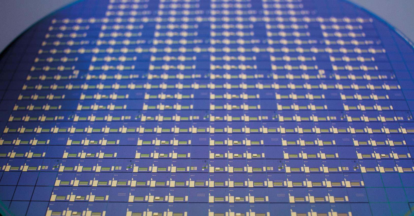
Manufacturing meritsThe strengths of our platform are not limited to its performance, but extend to its suitability for broad applicability, high-volume manufacturing and large-scale deployment. These advantages are partly due to a production process that realises high yields, thanks to low device sensitivity to process variations. However, there are additional merits of our technology. It is capable of integrating a large number of components at a high density; it produces low optical loss interfaces; and III-V materials are integrated in an efficient manner. What’s more, data throughput densities can exceed 200 Gbit/s/mm, due to our high-speed, compact, low-power modulator and detector technologies and interface electronics; and fibre coupling losses can be less than 1 dB with our simple, high-yield, high-throughput fibre attach assembly.
Using a complex manufacturing flow that involves many partners, we have also developed and implemented analogue, digital and mixed-signal electronics design and integration. This has enabled us to ship complete photonic chips and chipsets to serve different market sectors.
Ideally, silicon photonic chips form part of a set of wider technologies, together with CMOS, BiCMOS and packaging. We are able to incorporate all of these in a complete chipset, making our multi-micron silicon PIC platform a strong candidate in many markets.
One of these markets is data communications, where there is a rising global appetite for data-centre bandwidth. This is driving demand for in-package optics which involves integrating fibre-optic links with ICs. To enable edge integration, these ICs require high-bandwidth, compact PICs operating at more than 200 Gb/s/mm, a specification we can satisfy.
In addition, there is a need to keep pace with increasing bandwidth capabilities of switch ASICs, by scaling PIC modulators and detectors to higher data rates, while increasing their integration density. Our modulators and detectors are ideal for this task. Using our platform, transceiver PICs are smaller than 30 mm2 – that is comparable to, or smaller than, those made using sub-micron photonic platforms.
With an optical power handling capability of over 2 W, our multi-micron platform is also well suited to sensing applications, such as 3D imaging and LiDAR. These applications can involve the transmission of large optical powers, and require fast, steerable, narrow beams for high resolutions at high frame rates. One strength of our platform is its demonstrated capability to implement coherent receivers, an essential ingredient for frequency-modulated continuous wave LiDAR. This advanced form of LiDAR collects 3D imaging and velocity measurements – data that is much sought after by those developing advanced driver-assistance systems and related autonomous technologies for the automotive and transport markets.
Another strength of our platform is its high light confinement. This allows many emitters to fit on a tight pitch, aiding design of optical phased arrays, which can provide fast steering when equipped with waveguide diodes with response times of 10 ns or less.
Using our technology, we have demonstrated a high level of integration with many photonic devices including: compact arrayed waveguide grating filters, hybrid lasers, and high-speed modulators and detectors. Our platform’s versatility, combined with the physical benefits it brings, enables our technology to target many applications, from data communications to sensing. Competitiveness in these sectors is assured, because we are able to leverage a key success factor that microelectronics also enjoyed: the ability to deliver economies of scale with high-volume manufacturing made possible by multi-market technology applicability.


