Optical communications: Supporting colossal growth with superior lasers
As lasers with traditional architectures are helping to deliver ever
higher data rates, newer designs with even more impressive
characteristics are promising to gain traction.
BY RICHARD STEVENSON, EDITOR, CS MAGAZINE
There are times when anecdotal evidence obscures the big picture. That, though, is rarely the case. Take the youth of today – they have little interest in watching TV, but when the mood takes them they devour hour-after-hour of video clips on their devices. So, based on this observation, it is anything but surprising when market analysts forecast that the global transfer of data is on a continuous rise that shows no sign of abating.
Supporting the watching habits of the young, as well as the lives of all of us, is a rather complex infrastructure that enables the transmission of an astonishing level of data, involving systems working in both the RF and the optical domain. The capability of both is on the rise. For the RF, there’s the roll-out of 5G, while capacity of optical communication is increasing through the combination of sources with faster data rates and the laying of more fibre.
Like many of its predecessors, at this year’s European Conference on Optical Communication (ECOC) many speakers described efforts to hike data rates with optical technologies. This included the use of more sophisticated modulation schemes for propagating light through an optical fibre – a collaboration between researchers in Japan and Europe unveiled communication at an eye-watering 22.9 Pbit/s by extreme space-wavelength multiplexing – as well as increases in the modulation rate of many forms of laser. And in addition to the traditional approach to data transfer, involving optical fibre, a number of forms of free-space communication were discussed. They included transmission of data from Earth to satellites with 100 W sources emitting at around 1.55 µm, the use of blue and green lasers for underwater communication, and turning to light for the final link in homes and offices. Note that in many applications, one of the key benefits of switching from the RF to the optical is the far higher bandwidth.

Speaking in the Market Focus session, Coherent’s CEO Julie Eng gave an
excellent overview of the deployment of various forms of laser in
optical communications.
At the heart of all these forms of optical communication is the laser. In some cases, this device is directly modulated to deliver the data, and at other times it’s combined with some form of modulator.
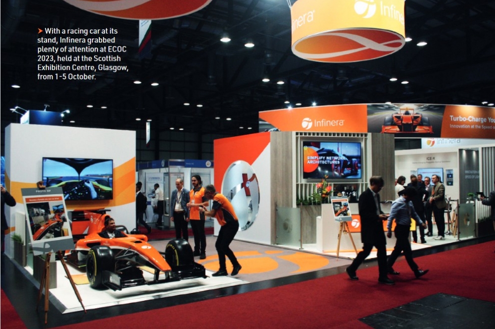
Those attending ECOC 2023 got to hear a great deal about this vital source of light. In the Market Focus session, held in the exhibition hall, volumes of various forms of laser used in optical communication were discussed by Julie Eng, CTO of Coherent; and Gunter Larish, Product Manager Datacom at Trumpf, spoke about VCSELs for interconnects at more than 100 Gbit/s. Meanwhile, in the conference sessions, Chang Ge from Tokyo University of Technology claimed a record-breaking speed for 1060 nm VCSELs with a metal aperture; and Takuro Fujii from NTT Device Technology Labs, Japan, outlined efforts at developing a directly modulated membrane laser array on silicon. Another novel laser taking prominence at ECOC was the PCSEL, short for the photonic crystal surface emitting laser. Its trailblazer, Vector Photonics, discussed the capabilities of this source in the Market Focus session, the conference, and an off-site meeting held at the company’s headquarters – this is just a short drive from the Scottish Exhibition Centre, the location for this year’s ECOC.
A Coherent overview
One of the biggest suppliers of lasers to the optical communications market is Coherent. Speaking on its behalf, Eng explained that sales of transceivers are undergoing tremendous growth, while life cycles are typically just 2-3 years. More than half of the products sold today are operating at 200 Gbit/s or more, a sector that will be worth $10 billion by 2028.
The Coherent CTO also offered an insight into the types of materials that dominate, and where they are used. She explained that InP dominates optical communications, accounting for around three-quarters of the market. Of the remainder, GaAs has the largest share, with silicon photonics responsible for just a few percent.
According to Eng, GaAs lasers, in the form of the VCSEL, are widely used in short-reach links of less than 100 m. Meanwhile, technologies based on InP and silicon photonics are deployed for transmission over 500 m to 10 km, and also at more than 10 km, where narrow laser linewidths are needed.
Eng remarked that the GaAs VCSEL is only capable of low powers, but at low cost, and its sales will benefit from the rise in AI and machine learning. Modulation speeds for this class of VCSEL are increasing, with 1 x 4 and 1 x 8 arrays providing 400 Gbit/s and 800 Gbit/s sources. There is now much interest in a 200 Gbit/s VCSEL. “We and the rest of the industry will be working on that,” added Eng.
For silicon photonics, which offers modulation and routing, there’s a need to combine this chip with a high-power InP laser. Options include 100 mW uncooled and 200 mW cooled sources, according to Eng.
Similar capabilities may be provided with electro-modulated lasers, produced using monolithic integration. Coherent has demonstrated 200 Gbit/s per lane, using a source with 7 dBm (5 mW) of power that’s claimed to be suitable for transmitting data over distances from 500 m to a few kilometres.
For longer distances, Eng advocates combining an InP laser emitting in CW with a Mach-Zehnder modulator, a pairing that offers 200 Gbit/s per lane. She encouraged delegates to go to a live demo of this at the Coherent booth, where data transfer took place over 6 km of fibre.
VCSEL virtues
VCSELs are now a high-volume product, with billions shipped every year, partly due to their incorporation in cell phones. The performance of this class of laser continues to advance, with the VCSELs of tomorrow expected to combine an increased channel capacity with reduced power consumption and enhanced functionality, according to Larish.
The spokesman for Trumpf told those attending the Market Focus session that his company has been developing VCSELs for many years, and is currently working on increasing the spectral range of this device beyond 850 nm to 880 nm, 910 nm, 940 nm, 980 nm and 1060 nm, for sources operating at 100 Gbit/s. Larish added that the company is already shipping VCSELs with data rates of up to 56 Gbit/s.
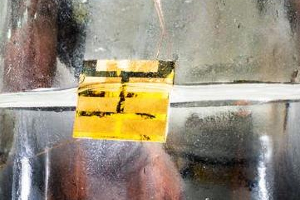
Significant progress in combining higher speeds with longer wavelengths, which increase the transmission distance and minimise dispersion, was claimed by Ge, who has been working with colleagues at the University of Tokyo and Ambition Photonics. This team has been advancing VCSELs with a metal aperture, a design that is said to increase bandwidth and improve temperature stability (see Figure 1).

Figure 1.The metal aperture VCSELs with surface relief, produced by the
University of Tokyo and Ambition Photonics, are capable of
record-breaking data rates.
The devices made by Ge and colleagues were fabricated using a surface relief process, involving shallow wet etching to a depth of 30 nm. The team applied this approach to 3-inch epiwafers featuring four InGaAs quantum wells, and top and bottom distributed Bragg reflectors (DBRs) formed with six and 30 mirror pairs, respectively. Confinement of the optical modes is realised with an oxide aperture, typically 5 µm in diameter, and a ring-shaped p-contact metal with a diameter of 5 µm, grown on the top DBR. A five pair dielectric is deposited on top of this, and a thick layer of polyimide inserted under the p-type pad to reduce parasitic capacitance and increase the modulation bandwidth.
This design provides enhancement of the bandwidth while controlling the transverse mode. Benefits come from the shorter resonance wavelength in the surface relief region, compared with the un-etched region, that allow the optical field to laterally spread into the oxidised region and reflect at the metal-aperture boundary.
Driven at 6 mA, these VCSELs produce a single-mode power of more than 2.5 mW. The divergence angle is 13 degrees, which is “almost the diffraction limit”, said Ge.
She shared the results of small signal characterisation at drive currents of 6 mA to 8 mA. “The record modulation bandwidth of over 31 GHz at a bias current of 8 mA was obtained for 1060 nm single-mode VCSELs, thanks to the coupled cavity effects” claimed Ge.
When coupling the emission from the VCSEL into a 2 km length of fibre with a small diameter, modulation bandwidth increased to 35 GHz, thanks to pulse compression. The product of the data rate and the link length is 450 Gbit/s km, claimed to be the highest value ever reported for a VCSEL.
“Recently, we demonstrated the record baud rate of over 128 Gbit/s over 2 km fibre transmission with non-linear DSP operation,” added Ge.

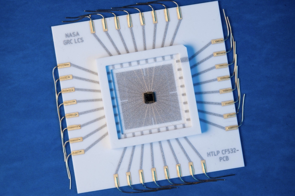
Figure. 2. The array of 16 InP membrane lasers by NTT Device Technology Labs has been developed with the aim of reducing the power consumed by data centres.
Frugal membranes
As well as helping to meet the demand to transmit ever more data, the lasers of tomorrow need to set a new benchmark for efficiency, to prevent the internet from accounting for an increasingly large carbon footprint. Discussing this matter, NTT researcher Fujii began his presentation by remarking that between 1 and 2 percent of global electrical consumption is associated with the data centre. Note that his company is targeting carbon neutrality for data centres by 2030.
To help produce more frugal data centres, Fujii and his research group have identified three objectives for next-generation devices. These aims, which encompass the need for greater efficiency and include other important requirements, are: a low power consumption, realised with a directly modulated laser with a low active volume; a low assembly cost, aided by the uptake of photonic integrated circuits produced using silicon process technologies; and a small footprint, due to the limited space for components.
“To meet these requirements, we are developing a membrane directly modulated laser on silicon,” explained Fujii. “The device consists of a membrane structured laser, together with a spot size converter, so that efficiency coupling to the fibre is achieved.”
He emphasised that one of the key features of this device is the thinness of the membrane structure – it is around just 350 nm thick (see Figure 2 for details of the device architecture). This InP-based structure is sandwiched between low-refractive-index SiO2 materials, leading to a high optical and carrier confinement that helps to reduce the device’s power consumption. Above the active region is a grating that ensures single-mode operation with a short cavity, another asset for trimming power consumption.
“Since we fabricate these lasers on silicon, the process can be scalable and we can use large silicon wafers to fabricate these lasers,” said Fujii. He added that in future, they could integrate several passive silicon photonic devices with their lasers.
Fabrication of the membrane lasers begins by growing an InP-based heterostructure, plus an etch-stop layer, on an InP substrate that is subsequently bonded to a SiO2-on-silicon wafer.
The InP substrate is then removed, before defining a mesa strip and forming a buried heterostructure with the regrowth of InP. n-type and p-type doping layers are then defined by thermal diffusion of zinc and ion implantation of silicon.
Fabrication is completed with the formation of an InP taper by etching, and the addition of a spot-size converter, created by deposition and etching of SiO2.
“The key point of our fabrication procedure is to carry out epitaxial growth after heterogeneous integration,” explained Fujii. “Why do we use such a unique fabrication procedure? It’s because it makes it possible to easily align the devices to the silicon photonic devices in the future.”
One downside of membrane lasers is the thermal strain between the InP-based and the silicon-based structures, due to differences in the coefficients of thermal expansion and the high temperatures required for MOCVD growth. Consequently, to supress thermal degradation, the InP-based heterostructure must be no more than 430 nm-thick, a value described as the critical thickness.
NTT have used their technology to develop a number of different devices, including lasers, modulators and photo-detectors. At this year’s ECOC, Fuji described the fabrication of a 16 channel directly modulated laser array, featuring 100 mm cavities and a low-loss spot-size converter.
One of the advances in this latest array, compared with previous devices, is the introduction of a non-alloy contact. This enables a smaller differential resistance and better uniformity.
To characterise the array, Fujii and co-workers applied an RF probe and coupled the output from the laser to a high-numerical aperture fibre using index-matching oil. They found that the lasers produced single-mode emission, and had a threshold current below 1.3 mA and a maximum output power of more than 1 mW. Wavelength variability for the lasers is less than ± 0.2 nm.
The team realised a date rate of 56 Gbit/s at both room temperature and 50 °C when transmitting over 2 km of fibre using 28 GBaud PAM 4 with a 9-tap simple linear equaliser. The transmission had an associated bandwidth density of 807 Gbit/s/mm and an energy cost of 0.65 pJ/bit. Encouragingly, the engineers found no electrical crosstalk between the channels when using a multi-channel RF probe.
Higher data rates were realised by turning to 56 GBaud PAM. This enabled transmission over 2 km of fibre at 112 Gbit/s at room temperature, but required an increase in the number of taps.
“We’ve also confirmed all 16 channel eye-diagrams, with a received output power of about 0 dB m,” said Fujji, who added that the bandwidth density and energy cost associated with this transmission were 1.6 Gbit/s/mm and 0.33 pJ/bit.
The power of the PCSEL
The capabilities of the PCSEL were championed at Vector’s headquarters by its Sales and Marketing Director, Euan Livingston. He explained that the Scottish start-up is on a mission to commercialise 2D PCSEL, which offer a level of functionality that is not possible with other lasers. The PCSEL combines surface emission with high speed, high power and a low cost.
Another great attribute of the PCSEL is its capability to emit an incredibly broad range of wavelengths. Any material that offers optical gain can be used to make a PCSEL. Vector has demonstrated devices with emission from 739 nm to almost 5 µm, using a a design with a quantum cascade laser structure to reach far into the infra-red.
Vector is a fabless company that will draw on a scalable supply chain to ramp up volumes of its devices. For the development of the VCSEL, the company has been well served by Scotland’s photonic cluster, which generates annual sales totalling $1.25 billion. Livingston feels that such success fails to get the recognition it deserves, arguing that more attention is given to photonics revenues for Wales, even though that is notably smaller.
During its initial PCSEL development, Vector has been using a local supply chain, with all its partners within 25 miles of its facilities. That’s a tremendous benefit, argues Livingston, because if issues arise, engineers can visit production sites, help to identify any problems and support the solutions. For prototyping, Vector has worked with: III-V Epi, to supply the epiwafers; Kelvin Nanotechnology, a provider of front-end processing; Helia Photonics, which supplies back-end-of-line services; and packaging expert Alter Technology. As volumes increase to tens of wafers per month, Vector may need to introduce new partners.
The timing of Vector’s launch was far from ideal, with the company formed on 13 March 2020, just days before the UK went into lockdown. This led to efforts to secure funding through on-line meetings, an approach that hampers efforts to build a rapport, but did not prevent Vector from raising significant investment. Innovate UK has provided financial support every year, with an initial investment of £2 million followed by £0.7 million in 2021, £2 million in 2022, and another £1 million in 2023. Alongside this £5.7 million, another £4.1 million has been raised from private equity. The company is now in the process of trying to secure additional investment, designed to support the company through to the end of 2024.
One of the big challenges facing Livingston and his fellow executives is determining which sector to pursue with their PCSELs. This class of laser is a promising alternative for deployment in many applications, and it could be used in cars, phones, computers, the internet and 3D printing. Vector’s leaders considered the opportunity associated with lidar, but found that the market for lasers was only worth $100 million, so looked elsewhere.
Now they expect the communication sector to provide the opportunity to ramp production and revenue, with the PCSEL supporting data rates of 800 Gbit/s and 1600 Gbit/s. Vector has identified 15 customers operating in this sector with very similar requirements. According to Livingston, the DFB lasers that serve in this application are limited to output powers of 100 mW or so, while the PCSEL can go far higher.
As well as evaluating and refining prototypes and evaluating market opportunities, Livingston and his colleagues are devoting much effort to securing their intellectual property, with meetings with patent lawyers on a weekly basis. Despite the high cost, Vector is filing patents. Initially they are filed in the UK, before the US, Europe and Japan.
The need to protect IP on a global scale reflects the worlwide production of III-V lasers, a device well represented at ECOC. There continues to be much progress in both the manufacture and development of these vital light sources for optical communication, with breakthroughs sure to feature at next year’s meeting, the fiftieth conference in this series, which will be held in Frankfurt from 22 to 26 September.