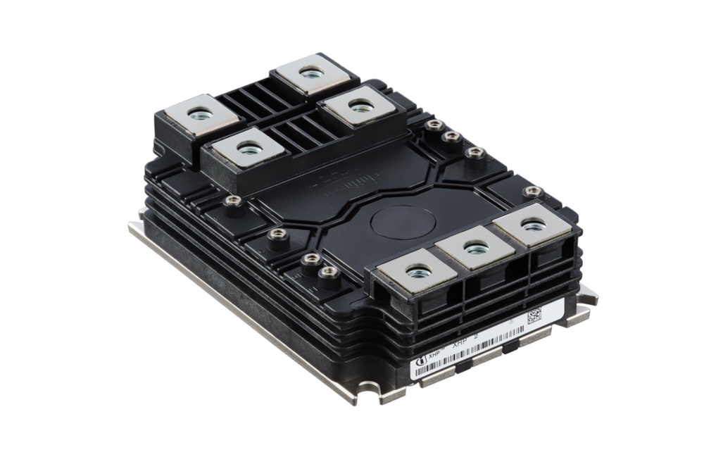
New 650V CoolSiC MOSFETs boost power density
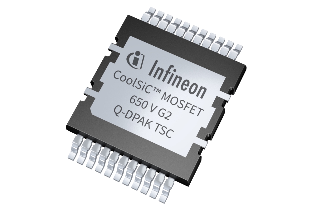
Infineon Technologies is expanding its portfolio of discrete CoolSiC MOSFETs 650V with two new product families housed in Q-DPAK and TOLL packages.
These diverse product families, with top- and bottom-side cooling, are based on the CoolSiC Generation 2 (G2) technology and use said to offer significantly improved performance, reliability, and ease of use.
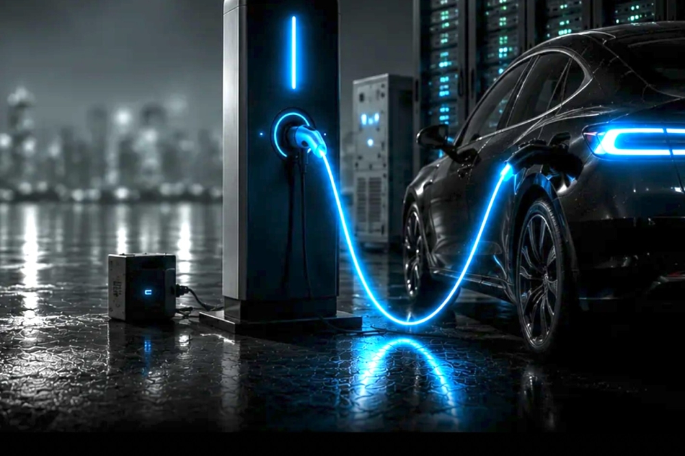
Applications includ high- and medium-power switched-mode power supplies (SMPS) including AI servers, renewable energy, chargers for electric vehicles, e-mobility and humanoid robots, televisions, drives and solid-state circuit breakers.
According to Infineon, the TOLL package offers outstanding Thermal Cycling on Board (TCoB), enabling compact system designs by reducing the PCB footprint. When used in SMPS, it can also reduce system-level manufacturing costs.
The introduction of the Q-DPAK package complements the ongoing development of Infineon's new family of Topside Cooled (TSC) products, which includes CoolMOS 8, CoolSiC, CoolGaN and OptiMOS.
The TSC family has been designed to help customers achieve excellent robustness with maximum power density and system efficiency at low cost. It also enables direct heat dissipation of 95 percent, allowing the use of both sides of the PCB for better space management and reduction of parasitic effects.
The CoolSiC MOSFETs 650 V G2 in TOLL are now available in R DS(on) from 10 to 60 mΩ, while the Q-DPAK variant is available in 7, 10, 15 and 20 mΩ.