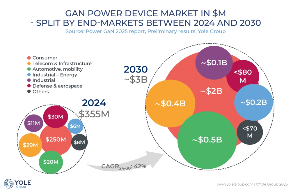
News Article
Enhancing mobility with mist CVD
Depositing the gate oxide of GaN MOSFETs by mist CVD delivers a hike in field-effect mobility
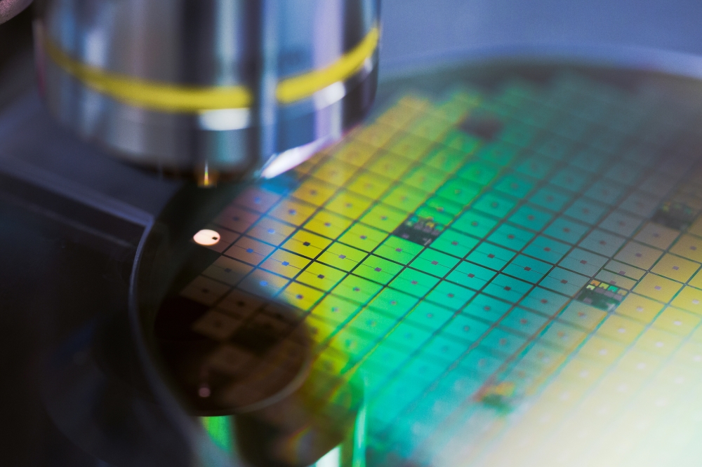
Sales of SiC MOSFETs are soaring, because they extend the driving range of electric vehicles by delivering a higher switching efficiency than silicon equivalents. Strengths of these vertical transistors include a high threshold voltage and a high current-handling capability, but losses are not as low as they might be, due to a channel mobility of around just 100 cm2 V-1 s-1.
However, this limited mobility could be addressed by turning to GaN MOSFETs with a SiO2 gate oxide grown by mist CVD, according to a partnership between Mirise Technologies and Kochi University of Technology. According to recent work by this team from Japan, GaN MOSFETs produced with this deposition technology combines a high threshold voltage with a mobility of more than 250 cm2 V-1 s-1.
For GaN MOSFETs, another requirement is a high threshold voltage, as this ensures that if these devices were deployed in inverters in electric vehicles, they would provide fail-safe operation. Spokesman for the team, Kauki Miyake, told Compound Semiconductor that data sheets for SiC MOSFETs reveal a threshold voltage of around 4 V for this device, leading one to assume that a similar value is needed if a GaN variant is to be competitive.
Miyake and co-workers are not the first to investigate the mobility of GaN MOSFETs. Previous studies have shown that GaOx at the interface impacts GaN MOSFET mobility, and the thickness of this oxide is influenced by the gases that are used, as well as the oxidation time and temperature. Earlier work also considered the channel mobility of GaN MOSFETs with SiO2 deposited by various techniques, but efforts to enhance mobility via oxidation control had limited success.
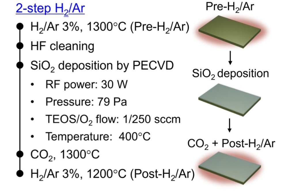
The researchers from Japan have addressed that issue, reducing GaN surface oxidation with plasma-enhanced CVD, atomic layer deposition (ALD), and mist CVD, which is a cost-effective method that does not require a vacuum system. In addition, the team have investigated the level of GaN surface oxidation in their samples, as well as measuring channel mobility and the interface state density.
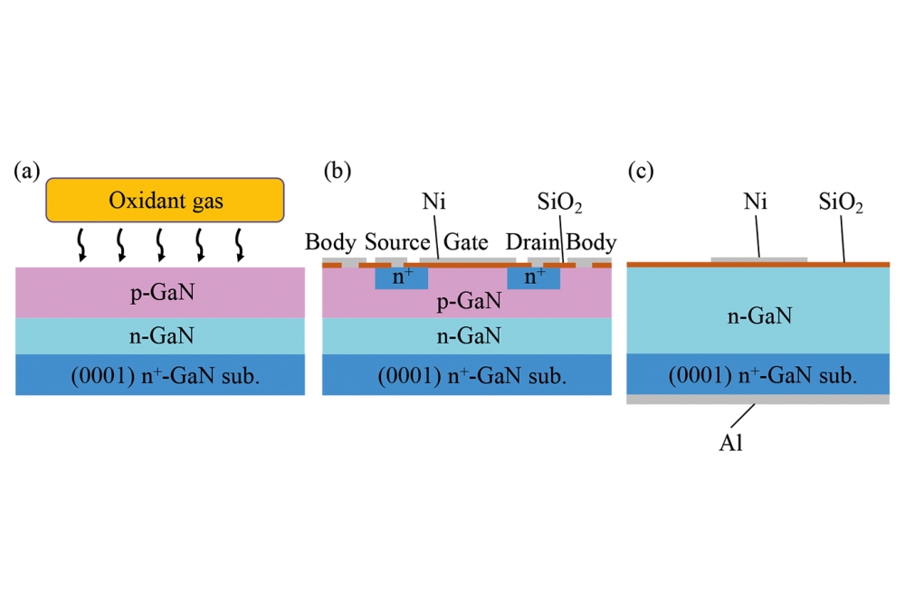
To assess the capability of all three deposition techniques, Miyake and co-workers have applied oxidant gas to epitaxial layers; produced lateral MOSFETs to assess channel mobility; and made n-type MOS capacitors, to determine the density of interface states (see figure).
Analysis of X-ray photoelectron spectroscopy offers an insight into the oxidation ratio of various samples under different oxidation conditions. For all three growth techniques, a long oxidation time increases the oxidation ratio. This ratio also increases within the ALD samples by moving from H2O to O3 and then to an O2 plasma.
Samples produced by mist CVD have a lower oxidation ratio than those produced by ALD using the same oxidation time and same oxidant gas, O3. The team attributes this to variations in O3 concentration, differences in the heater configuration in the deposition equipment, and variations in gas flow through the chamber.
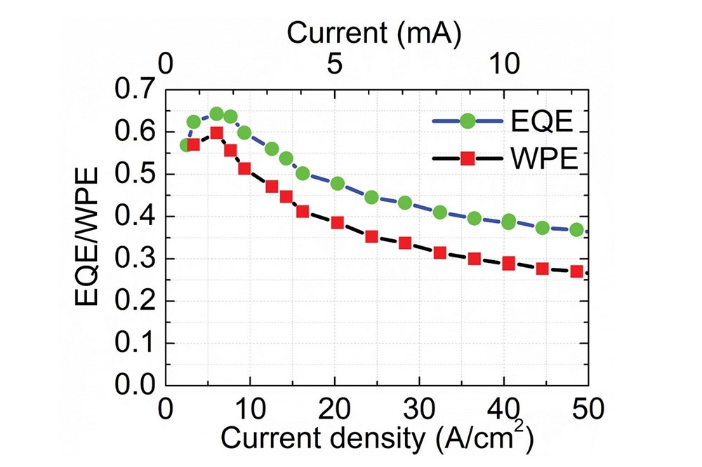
Measurements on the lateral MOSFETs reveal values for the threshold voltage, defined as the voltage at a current of 1 x 10⁻⁸ A, of 4.4 V for growth by plasma enhanced CVD, -9.0 V for ALD, and 4.8 V for mist CVD. The later technique, using O3, led to the highest field mobility of 266 cm2 V-1 s-1 – that’s more than twice that of the GaN MOSFETs produced by other techniques.
Scrutinising the interface of these lateral MOSFETs by cross-sectional scanning transmission microscopy, and applying electron-energy-loss spectroscopy, show that the nitrogen-to-gallium ratio decreased in the ALD-grown device at the interface of SiO2 and GaN, indicating the presence of thick GaOx. This technique also revealed that mist CVD using O3 is an effective SiO2 deposition method for supressing GaOx.
Plots of capacitance-voltage provided a value of just 8 x 1010 cm2 V-1 s-1 for the interface state density of the capacitor produced by mist CVD using O3. In comparison, values for capacitors produced by plasma-enhanced CVD and ALD were 1.2 x 1012 cm2 V-1 s-1 and 2.1 x 1012 cm2 V-1 s-1, respectively.
Miyake says that the team will now apply mist CVD to the fabrication of vertical GaN MOSFETs.
Reference
K. Ikeyamam et al. Appl. Phys. Express 17 064002 (2024)
Pictured above: Researchers from Mirise Technologies and Kochi University of Technology produced: (a), an epitaxial layer for oxidation evaluation; (b), a lateral MOSFET for determining channel mobility; and (c), an n-type MOS capacitor for finding the density of interface states.