
2D MoS₂ FPGA integrates 4000 FETs
2D transition metal dichalcogenides (2D-TMDs) are seen as promising candidates for future technology. However, current 2D-TMDs-based semiconductor devices are generally focused on simple logic circuits.
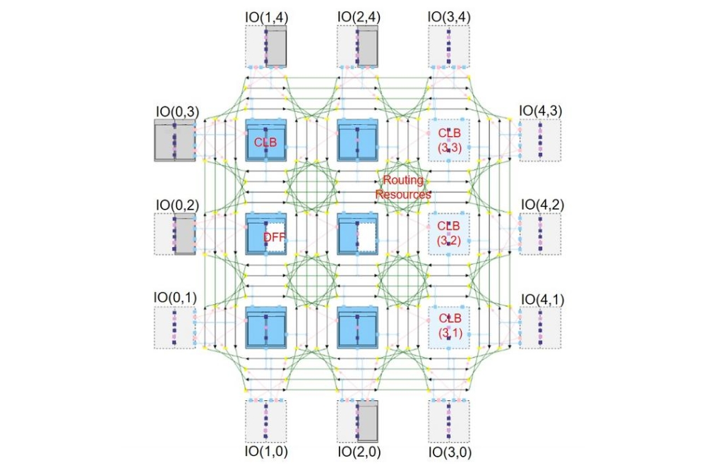
Now a Chinese team, led by Peng Zhou and Wenzhong Bao at Fudan University, has developed a top-gate (TG) 2D field-programmable gate array (FPGA) based on MoS2, comprising approximately 4000 FETs. In addition, they say the circuits demonstrate advantages in irradiation resistance.
They reported the work 'A field-programmable gate array based on wafer-scale two-dimensional semiconductor' in National Science Review.
The Fudan team used a wafer-scale 2D semiconductor integration process platform to overcome challenges associated with large-scale integration and yield control. The integration flow ensures reliable operation of the core logic units using only n-type transistors.
Furthermore, the chip’s configuration memory array, which dictates the logic functions, adopted a compact and efficient 2T0C DRAM structure. This design choice consumes significantly less chip area than traditional 6T-SRAM configuration cells commonly used in FPGAs, contributing to higher overall integration density.
Total ionising dose (TID) tests were conducted to rigorously verify the device reliability in extreme environments. The 2D FPGA successfully withstood exposure to 10 Mrad of gamma radiation while maintaining full functionality of the core logic modules.
This achievement provides a new materials-based technical route for developing high-reliability electronic components. Crucially, the intrinsic radiation resistance can significantly reduce the dependence on heavy external shielding layers currently required in critical systems for applications such as aerospace and high-reliability computing.
Using industry-standard design flows, the team successfully verified multiple complex digital logic functions on the same 2D FPGA circuit, including adders, multipliers, and counters.
The team plans to leverage its established core technology system and silicon-compatible integration processes to deepen collaboration with industrial partners, thereby accelerating the translation of these 2D chips from the laboratory environment into high-value markets.
A field-programmable gate array based on wafer-scale two-dimensional semiconductor
Reference
Qicheng Sun et al; National Science Review (2025)


