

KAIST finds clue to solving 'electrical bottleneck'
When the pathways through which electricity flows inside a semiconductor become blocked, device performance declines and power loss increases.
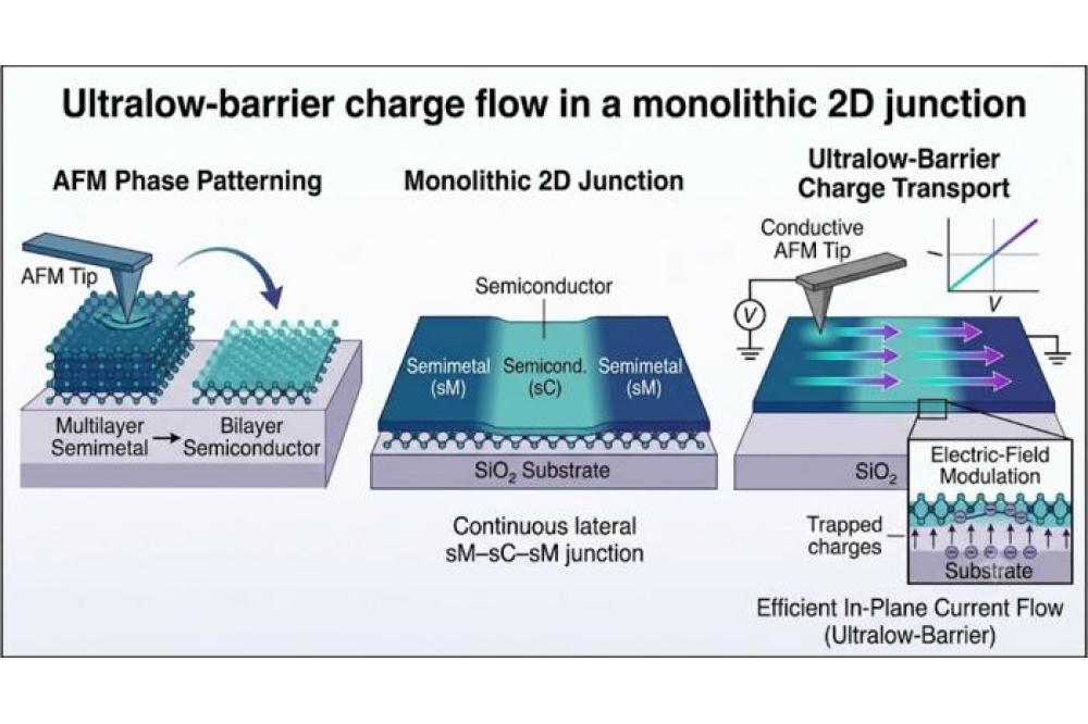
A Korean team of researchers from KAIST and Sungkyunkwan University has now developed a new structure that could resolve this 'electrical bottleneck' and, for the first time, directly confirmed that electric charges flow continuously without interruption.
Led by Seungbum Hong from the department of materials science and engineering KAIST, the team also developed an analytical platform capable of directly observing this charge transport at the nanometer scale.
Instead of attaching a metal electrode on top of a semiconductor as in conventional approaches, the research team continuously formed semi-metallic and semiconducting regions within a single thin film of 2D PtSe₂. By creating a structure in which the two regions are naturally connected within the same material, the team demonstrated that current can flow across the boundary without being blocked.
Using Atomic Force Microscopy (AFM),the team directly visualised charge transport inside the thin film at the nanometer scale.
Furthermore, the team verified device operation by applying an electric field to the semiconducting region. The results confirmed that current flow can be stably controlled in a metal–semiconductor junction structure, demonstrating the potential of the structure for next-generation electronic devices.
The work 'Nanoscale imaging of charge transport across the semimetal-semiconductor interface in monolithic platinum diselenide' was published in the July 2026 issue of Matter, an international journal in the field of materials science.



