
MIT team develops low cost GaAsP solar cell
A team of researchers from MIT and the Masdar Institute of Science and Technology has developed a new solar cell made by layering a GaAsP-based solar cell on a low-cost silicon solar cell..
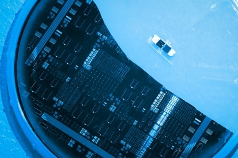
The researchers call the device a "˜step cell' because the two layers are arranged in a stepwise fashion, with the lower layer jutting out beneath the upper layer, in order to expose both layers to incoming sunlight.
Usually multijunction solar cells are typically expensive to manufacture, but the researchers also used a novel, low-cost manufacturing process for their step cell.
The team's step-cell concept can reach theoretical efficiencies above 40 percent and estimated practical efficiencies of 35 percent, prompting the team's principal investigators - Masdar Institute's Ammar Nayfeh, associate professor of electrical engineering and computer science, and MIT's Eugene Fitzgerald, the Merton C. Flemings-SMA Professor of Materials Science and Engineering - to plan a startup company to commercialise the promising solar cell.
The team presented its initial proof-of-concept step cell in June at the 43rd IEEE Photovoltaic Specialists Conference in Portland, Oregon. The researchers have also reported their findings at the 40th and 42nd annual conferences, and in the Journal of Applied Physics and IEEE Journal of Photovoltaics.
Beyond silicon
Layered solar cells can reach theoretical efficiencies upward of 50 percent, but their very high manufacturing costs have relegated their use to niche applications, such as on satellites, where high costs are less important than low weight and high efficiency.
The Masdar Institute-MIT step cell, in contrast, can be manufactured at a fraction of the cost because a key component is fabricated on a substrate that can be reused. The device may thus help boost commercial applications of high-efficiency, multijunction solar cells at the industrial level.
The silicon layer is exposed, appearing like a bottom step. This intentional step design allows the top GaAsP layer to absorb the high-energy photons (from blue, green, and yellow light) leaving the bottom silicon layer free to absorb lower-energy photons (from red light) not only transmitted through top layers but also from the entire visible light spectrum.
"We realized that when the top GaAsP layer completely covered the bottom silicon layer, the lower-energy photons were absorbed by the silicon germanium - the substrate on which the gallium arsenide phosphide is grown - and thus the solar cell had a much lower efficiency," explains Sabina Abdul Hadi, a PhD student at Masdar Institute whose doctoral dissertation provided the foundational research for the step-cell. "By etching away the top layer and exposing some of the silicon layer, we were able to increase the efficiency considerably."
Working under Nayfeh's supervision, Abdul Hadi conducted simulations based on experimental results to determine the optimal levels and geometrical configuration of the GaAsP layer on silicon to yield the highest efficiencies. Her findings resulted in the team's initial proof-of-concept solar cell. Abdul Hadi will continue supporting the step cell's technological development as a post-doctoral researcher at Masdar Institute.
On the MIT side, the team developed the GaAsP, which they did by growing the semiconductor alloy on a substrate made of SiGe.
"GaAsP cannot be grown directly on silicon, because its crystal lattices differ considerably from silicon's, so the silicon crystals become degraded. That's why we grew the GaAsP on the SiGe - it provides a more stable base," explains Nayfeh.
The problem with the SiGe under the GaAsP layer is that SiGe absorbs the lower-energy light waves before it reaches the bottom silicon layer, and SiGe does not convert these low-energy light waves into current.
"To get around the optical problem posed by the silicon germanium, we developed the idea of the step cell, which allows us to leverage the different energy absorption bands of GaAsP and silicon," says Nayfeh.
The step cell concept led to an improved cell in which the SiGe template is removed and re-used, creating a solar cell in which GaAsP cell tiles are directly on top of a silicon cell. The step-cell allows for SiGe reuse since the GaAsP cell tiles can be under-cut during the transfer process. Explaining the future low-cost fabrication process, Fitzgerald says: "We grew the GaAsP on top of the SiGe, patterned it in the optimised geometric configuration, and bonded it to a silicon cell. Then we etched through the patterned channels and lifted off the SiGe alloys on silicon. What remains then, is a high-efficiency tandem solar cell and a SiGe template, ready to be reused."
Because the tandem cell is bonded together, rather than created as a monolithic solar cell, the SiGe can be removed and reused repeatedly, which significantly reduces the manufacturing costs.


