
Munich team makes double helix inorganic semiconductor
A team from the Technical University of Munich (TUM) has made an inorganic semiconductor with a double helix structure. The highly flexible material, called SnIP, is a compound of tin, iodine and phosphorus that has both optical and electronic properties.
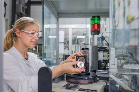
The centimetre-long fibres can be arbitrarily bent without breaking, a property attributable to the double helix, says Daniela Pfister (above), who discovered the material and works as a researcher in the work group of Tom Nilges, professor for synthesis and characterisation of Innovative Materials at TU Munich.
"SnIP can be easily produced on a gram scale and is, unlike GaAs, which has similar electronic characteristics, far less toxic," she says.
Application possibilities
The semiconducting properties of SnIP promise a wide range of application opportunities, from energy conversion in solar cells and thermoelectric elements to photocatalysts, sensors and optoelectronic elements. By doping with other elements, the electronic characteristics of the new material can be adapted to a wide range of applications.
Due to the arrangement of atoms in the form of a double helix, the fibres, which are up to a centimetre in length can be easily split into thinner strands. The thinnest fibres to date comprise only five double helix strands and are only a few nanometers thick. That opens the door also to nanoelectronic applications.
"Especially the combination of interesting semiconductor properties and mechanical flexibility gives us great optimism regarding possible applications," says Nilges. "Compared to organic solar cells, we hope to achieve significantly higher stability from the inorganic materials. For example, SnIP remains stable up to around 500degC."
"Similar to carbon, where we have the 3D diamond, the 2D graphene and the 1D nanotubes," explains Nilges, "we here have, alongside the 3D semiconducting material silicon and the 2D material phosphorene, for the first time a one dimensional material - with perspectives that are every bit as exciting as carbon nanotubes."
Just as with carbon nanotubes and polymer-based printing inks, SnIP double helices can be suspended in solvents like toluene. In this way, thin layers can be produced easily and cost-effectively. "But we are only at the very beginning of the materials development stage," says Pfister. "Every single process step still needs to be worked out."
Since the double helix strands of SnIP come in left and right-handed variants, materials that comprise only one of the two should display special optical characteristics. This makes them highly interesting for optoelectronics applications. But, so far there is no technology available for separating the two variants.
Theoretical calculations by the researchers have shown that a whole range of further elements should form these kinds of inorganic double helices. Extensive patent protection is pending. The researchers are now working intensively on finding suitable production processes for further materials.
Interdisciplinary cooperation
An extensive interdisciplinary alliance is working on the characterisation of the new material: Photoluminescence and conductivity measurements have been carried out at the Walter Schottky Institute of the TU Munich. Theoretical chemists from the University of Augsburg collaborated on the theoretical calculations. Researchers from the University of Kiel and the Max Planck Institute of Solid State Research in Stuttgart performed transmission electron microscope investigations. Mössbauer spectra and magnetic properties were measured at the University of Augsburg, while researchers of TU Cottbus contributed thermodynamics measurements.
The research was funded by the DFB (SPP 1415), the international graduate school ATUMS (TU Munich and the University of Alberta, Canada) and the TUM Graduate School.
'Inorganic Double Helices in Semiconducting SnIP' by Daniela Pfister et al: Advanced Materials, Sept. 12, 2016


