
Bringing MBE to the masses
Can the 'Swiss Army knife of MBE tools' continue to seize market share as applications escalate, Compound Semiconductor asks Veeco.
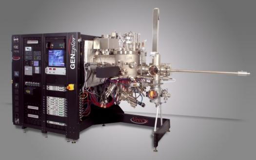
Veeco is poised to deliver its 25th GENxplor R&D molecular epitaxy beam system.
Unmasked in China, three years ago, Veeco's research and development MBE system, 'GENxplor' has since reached worldwide acclaim.
Twenty five systems will soon be up and running in universities and research institutions around the globe, and Veeco vice president of MBE products, Gerry Blumenstock, expects the next three years to bring more of the same.
"We launched the tool at China MBE 2013 as we could see lots of investment was being put into growing China-based universities and technologies, and leading [industry players] had moved out to China," he says.
"But while we've recently won business in China, system adoption has been pretty universal," he adds. "Annual sales are tied to research and development funding and I don't see the annual number of MBE tool sales changing."
The GENxplor system deposits epitaxial layers on substrates up to three inches in diameter and, to date, has been used for a vast number of III-V materials systems for myriad applications including high speed transistors, 2D materials research and UV-LEDs.
Veeco itself manufactures a fleet of MBE research and production tools for structure and device fabrication on larger four and six inch substrates. But as Blumenstock highlights, this instrument's single-frame design comprises vacuum hardware and on-board electronics, making it up to 40% smaller than other MBE systems. "It's like we made this the Swiss Army knife of MBE tools," he says.
Veeco's first sale came from the University of Oklahoma, with researchers developing materials for lasers, photodetectors and solar cells. From here, sales continued along the East and West coasts of the US, spread out to Europe, with China coming on board in the last twelve months.
And right now, the development of RF devices for mobile phones across Asia - especially in China - is a leading light for sales of this MBE system.
"Historically, western suppliers have been used for critical epilayer growth but now we're seeing domestic Chinese suppliers acquiring this technology to produce devices for domestic consumption," highlights Blumenstock. "This is a big shift."
And while the company vice president emphasises that sales stem from a 'constellation of applications all over the world', he is excited about the opportunities the growing UV-LED market brings. "We have UV-LEDs earmarked as an application that could require larger, production tools," he says. "It's still early days and companies are emerging but... look at end market applications such as water purification and UV curing."
"These are such big applications and the UV-LED provides low power consumption and high overall power output; so to me, this feels like it could be big for our industry," he adds.
Rival technology
However, it's no secret that many device manufacturers favour MOCVD over MBE for epitaxy layer deposition. Indeed, according to Blumenstock, MOCVD is mass production friendly with the market volumes of this type of tool dwarfing MBE systems, for say, GaN applications.
But, as he highlights, Veeco itself develops both MBE and MOCVD systems, and as such, will supply what a customer wants. "The choice depends on the end-customer and what they are looking for," he says. "Some customers will always find a way to make MOCVD work while others will choose MBE as they feel they really can't use anything else."
"Certain designs of UV-LED structure require a high Aluminium content and we see these being preferentially made using MBE but we represent both technologies and take the stance that we supply what suits you," he adds.
So with the 25th sale of GENxplor secured, where next? The company is currently working on a new suite of sources for its fledgling MBE system. Blumenstock claims company researchers have made breakthroughs in source stability and component lifetime, which will soon be introduced to systems.
"Researchers and manufacturers will be able to increase production yields and also [develop] more complex devices and stacks for higher performing optical and electronic devices," he says. "We're pretty excited about that."


