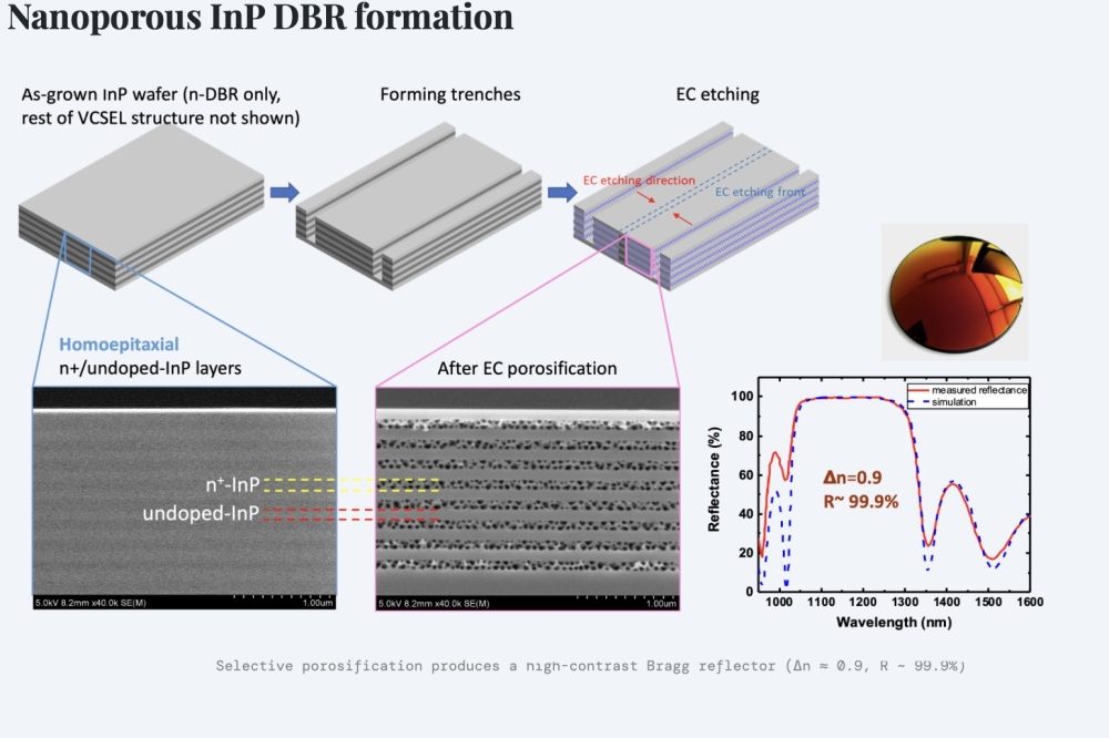
Say hello to the heterogeneous revolution

Recent advances in circuits produced by heterogeneous integration highlight the potential for real world applications.
BY CHRISTOPHER MAXEY, JUSTIN KIM, DAVE HODGE, MARK SOLER, BENNETT COY, DAN GREEN, JAMES BUCKWALTER AND FLORIAN HERRAULT FROM PSEUDOLITHIC INC.
Since the advent of VLSI silicon CMOS, this technology’s RF and millimetre-wave performance has taken a back seat during the inexorable drive towards smaller gate dimensions and higher device density. Stepping up to fill this gap have been a number of compound semiconductors, such as GaAs, GaN, and InP, providing high gain and high output powers at ever higher frequencies. Thanks to these devices, it has been possible to construct solid-state phased-array radars, 5G/6G base-stations and quantum computers. However, these applications pay a significant price in an ecosystem where many may see ‘exotic’ materials as an issue that slows and restricts adoption. Compared to silicon CMOS, it typically takes twice as long to fabricate compound semiconductor devices, which are 5 to 10 times as expensive per unit area, because they lack the fundamental economic benefits of high-volume manufacturing.

Figure 1. Silicon CMOS and compound semiconductors provide unique benefits, while heterogeneous integration promises to deliver the best of both worlds.
One attractive solution to addressing this issue is heterogeneous integration. Many are now investigating this approach that combines the disparate benefits of multiple technologies into a single integrated circuit (see Figure 1). Here, we review the rise in interest in heterogeneous integration, its progress in the context of the historical evolution of semiconductor technologies, and the potential inflection it offers to accelerate deployment of new devices into the marketplace. We also describe the contribution that our company, PseudolithIC, is making – we are the pioneers of a number of ‘first-ever’ prototype designs, including the world’s first millimetre-wave amplifier based on InP and GaN devices.
HI primed for impact
Evidence of accelerating interest in heterogeneous integration is found in increases in journal articles and patent filings over the last three decades (see Figure 2). At the turn of the millennium heterogeneous integration started to take shape as a bone fide topic, and since then there has been a steady rise in publications continuing to the present day. Alongside this trend, there has been a multiplication in both the number of potential approaches to realising integrated solutions, and the potential applications for heterogeneous integration. For example, integration of varying digitally focused chiplets has spawned multiple conferences and consortia, including the recent Universal Chiplet Interconnect Express consortium. Supporting and spurring on much of this activity are federally funded efforts, such as the DARPA CHIPS programme. There are also many efforts driven by government research programmes that focus on mixing optical technologies at the chip scale to trim the cost and improve the performance of photonic integrated circuits.

Figure 2. Articles and patents referencing heterogeneous integration over five-year periods spanning the 1970s to today. The final period includes a linear extrapolation for the remainder of the current period (courtesy Google Scholar).
Looking more broadly at the history of semiconductor innovation, the timeline from a technology’s first results to its commercial deployment has consistently been on the order of two decades. The time that it takes to develop a compound semiconductor device technology, such as that based on GaAs or GaN, is very similar to that for silicon (see Figure 3), with initial device results preceding deployment in commercial applications by about 20 years.
For both GaAs and GaN, development has been facilitated by significant industrial investment, underwritten in part by the US Government. Development of GaAs devices has been supported by the DARPA MIMIC programme, while advances in GaN have been aided by the DARPA WBGS programme. Heterogeneous integration is now on the cusp of commercial employment, and has benefitted from similar developmental investment. Based on historic rates of progress, we can conclude that heterogeneous integration is primed to realise its commercial impact.
Merits of the PseudolithIC approach
A number of research groups are focusing on RF applications, and exploring several approaches. We are involved in this area, but taking the technology much further, by commercialising a chip-scale 2.5D integration approach that leverages existing RF silicon and compound semiconductor ecosystems.
Our approach offers three critical value propositions over monolithic processes, which concentrate on a single material. First, we accelerate the design and fabrication process for a high-performance RF circuit. An example of this is designing new circuits and integrating exotic materials, such as N-polar GaN, faster than a traditional foundry, because we just require chiplets of the material, rather than an entire MMIC. Consequently, several thousand chiplets can be procured from a single tape-out (see Figure 4). Once we have sourced our chiplets and built up an inventory, our designers only need to design the interposer to produce a new pseudolithic IC, which we refer to as simply a PLIC. Second, our approach enables a true ‘mix-and-match’ of different devices, such as InP and GaN, in a single PLIC. This enables optimal architectures that are free from multi-chip modules. Finally, as the interposer is built on wafers with a diameter of at least 8 inches, they have at least four times the area of the 4-inch wafers used in typical III-V processes, leading to significant fab throughput and cost advantages.
To enjoy all these benefits, we employ an approach that begins by sourcing individual active III-V transistors – or even more complex integrated circuits – from either an established defence industrial base or a commercial foundry. After dicing these devices into singulated ‘chiplets’, they are embedded into a separately designed and fabricated silicon substrate interposer, which may feature passive networks, such as transformers, and active CMOS control circuity. By adopting a low-temperature process, we maintain the integrity of the chiplets and the in-situ CMOS devices. Our final step, completing integration at the wafer scale, is the fabrication of copper coplanar waveguide interconnects between the chiplet and interposer.

Figure
3. A timeline illustrating the evolution of silicon, GaAs, GaN and
heterogeneous integration as semiconductor technologies.
The finished product, a PLIC, is completely planar and compatible with commercial die attach, packaging, and chip-on-board processes, aiding downstream integration in higher-level systems. Critically, the PLIC is nearly indistinguishable from a single technology IC (see Figure 5, which shows a cross section of a PLIC after the chiplets are embedded in the interposer, and highlights the thermal advantages that result from direct access to the backside of the high-power chips).
First pass successes
Our unique process, which capitalises on the maturity and reliability of silicon to simplify the millimetre-wave and microwave MMIC design processes, results in an exceptionally high first-pass success rate. Exemplifying the advantages of our process are recent publications outlining how our technology can be used to produce an N-polar GaN power amplifier, an InP power amplifier, and a two-stage amplifier that features both InP and GaN technology.
Recent research shows that N-polar GaN HEMTs offer high-efficiency, high-power density, and excellent linearity for microwave and millimetre-wave applications. However, transitioning emerging GaN HEMT technologies into commercial applications is impeded by the lengthy foundry development cycle for a full MMIC process – this involves device maturation and qualification, and incurs a high cost, due to the specialised 4-inch epitaxial wafers. Our approach addresses some of these delays, with an acceleration of material to viability, thanks to the introduction of a heterogeneous design that embeds an N-polar transistor in a silicon interposer.
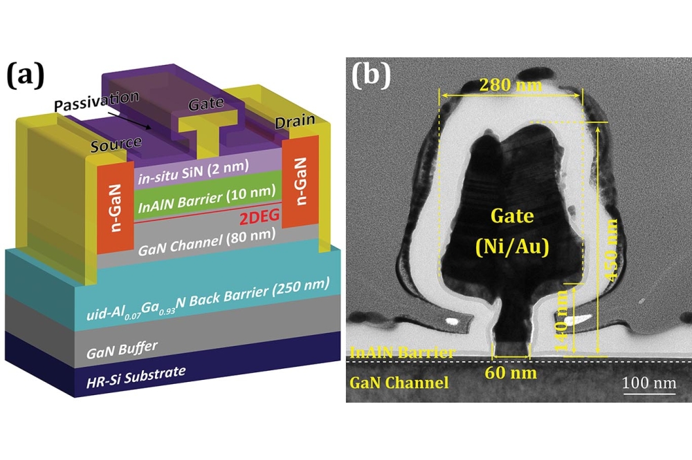
For the amplifier we have fabricated, we use a HEMT chiplet with: an 80 nm gate length; 500 nm gate-drain separation; and two fingers of 37.5 µm width, for a total gate periphery of 75 µm. Measurements of S-parameters for this amplifier suggest a peak output power of 150 mW (see Figure 6). Despite designing across two processes, there is excellent agreement between 20 GHz and 40 GHz, thanks to the maturity of our custom design environment that is adept at uniting silicon and III-V technologies. The peak gain of our amplifier reaches 8.0 dB at 26 GHz. At this frequency, the input and output return loss exceed 16 dB and 12 dB, respectively. The reverse isolation, S12, is better than 20 dB across the frequency band. The measured amplifier is unconditionally stable from 0 to 40 GHz.

Figure 4. Micrograph of an example ‘sea of transistors’ wafer used for N-polar GaN chiplet fabrication.
We have also demonstrated similar first-pass success with more mature process technologies, including a 250 nm InP HBT process reported in early 2024. This process offers a 2.5 V supply with a maximum oscillation frequency (fmax) approaching 650 GHz. The high value for fmax, and also for the cut-off frequency (fT), ensures that this technology is attractive for high-gain and high-efficiency blocks.
Additional attributes are a low supply voltage and a high collector current density of 2 mA µm-1, strengths that support matching that is closer to a desired 50 Ω. Due to this, a lower impedance matching quality factor (Q) is required to match to the device, leading to wideband amplifier designs.
Our heterogeneously-integrated InP amplifier, shown in Figure 6, has differential-mode stabilisation included on the chiplet. To allow supply of the base voltage through the common mode node, a transformer with capacitive isolation is used on the input. The differential signals on the collector are combined through a sub-quarter-wavelength balun on the output. Using this configuration, our amplifier exhibits 10.6 dB of gain at 24 GHz, with a total power consumption of only 45.3 mW.

Figure 5. Cross section of a completed PseudolithIC PLIC with a chiplet embedded in a silicon interposer.
Combining GaN and InP
Building on our foundation that has established that single III-V technology heterogeneous integration is viable and commercially competitive, we have gone on to prove that our technology can mix and match different III-V device types in the same integration process. For this demonstration, we have drawn on the success of our previous two circuit designs, by designing and fabricating a two-stage amplifier that has an InP first stage and a GaN second stage. The motivation for making this single PLIC is that no single technology is best suited for all RF functions. In our Ka-band amplifier, we need an InP first stage to maximise gain and a GaN second stage to maximise output power (see Figure 8 for a die micrograph of the fabricated PLIC and a top-level schematic of the two stages).
As we had previously built and tested each stage independently prior to this design, we concentrated our efforts on a new interstage matching network and making slight adjustments to the previous input and output matching networks. This again demonstrates how we can accelerate the adoption of heretofore impossible circuit topologies through our unique process. Our combined amplifier measures over 20 dB of gain at 25.7 GHz, validating our approach of merging the two technologies.

Figure 6. (top) Chip microphotograph of the 26 GHz heterogeneously integrated amplifier illustrating the compact implementation of the input and output matching networks. For clarity, the HEMT chiplet and interconnect are highlighted. (bottom) Simulated (dashed) and measured (solid) S-parameters of the heterogeneously integrated amplifier. A peak gain of 8.0 dB occurs at 26 GHz.
Higher levels of integration
Transmit/receive modules are ubiquitous in commercial and defence electronics. Here there is an ever-present demand for higher performance, realised at a lower cost and at higher frequencies. Defence electronics is tending to migrate to the V- and W-band to gain both bandwidth and a spectrum access advantage over potential adversaries. Similarly, commercial electronics are moving to higher frequencies, in this instance to satiate the growing demand for bandwidth in cellular and satellite communications networks. Heterogeneous integration is ideally suited to meet all these application requirements, providing an optimised performance in small form factors.
Conventionally, transmit/receive modules are constructed from multiple die, and packaged and interconnected with traditional PCB-style manufacturing techniques. This approach is adopted because no single monolithic process is ideal for each of the transmit/receive functions (see Table 1 for some of the design considerations for a typical transmit/receive module, including devices that best meet those requirements).

Figure 7. Chip micrograph of the Ka-Band heterogeneously integrated InP amplifier.
Building on our success with our multi-stage, multi-technology amplifier, we have designed and fabricated several generations of transmit/receive modules that mix different devices to achieve optimal performance in a very small form factor, typically around just 5 mm2. According to our latest simulations, our technology can deliver an output power of 2 W from the transmit path of the module. The receive path can deliver 12 dB of gain at 28 GHz while maintaining a total noise figure below 2.5 dB for the module when accounting for switch loss. There is no doubt that heterogeneous integration holds the key to realising an optimal technology combination, and enabling great performance from a small form.
Following 20 years of public and private investment and research activity, it appears that heterogeneous integration is now poised for commercial adoption, thanks to continued maturation and evolution of the foundational manufacturing techniques. We have contributed to this development with a proprietary process that has yielded several ‘first-ever’ prototype designs, highlighting the key benefits of heterogeneous integration for RF and millimetre-wave circuits.

Figure 8. High level schematic of the two-stage amplifier
(top) and a die micrograph of the fabricated device (bottom).
Our triumphs include the world’s first millimetre-wave amplifier that combines InP and GaN devices, a demonstration that underscores the extreme flexibility associated with combining different technologies. Another significant success is our dense transmit/receive module designs that combine InP, GaN and CMOS to deliver higher performance and lower cost. While this demonstration has targeted Ka-band applications, the approach extends readily to frequencies at W-band and beyond. These results highlight that the moment has now arrived to transition heterogeneous integration to various applications, from commercial 5G/6G telecommunications to defence electronics and beyond.

Table 1. Design considerations for a Ka-Band T/R module.