
3D-Micromac: a faster slice
Will novel wafer dicing slice up SiC in time for market growth, asks Compound Semiconductor.
Laser micromachining from 3D-Micromac: ready for action?
Read any recent analyst forecast and it's plain to see that silicon carbide power device businesses are poised for growth.
Recent reviews from France-based Yole Developpement predict the SiC power market will swell from some $200 million in 2015 to more than $550 million in 2021. And come 2025, IHS, US, reckons these figures will mushroom to $3 billion.
But while this spells good news for device manufacturers, worldwide, a manufacturing bottleneck is already looming in the form of wafer dicing. While today's state-of-the-art mechanical blade dicing tackles silicon and many other substrates with ease, SiC is a different beast.
As Hans-Ulrich Zuehlke, market development manager at Germany-based laser micromachining systems manufacturer, 3D-Micromac, points out, SiC is almost as hard as the diamond saw blade itself. As a result, mechanical dicing has to take place at low feed rates - from 2 to 10 mm/s - to minimise tool wear, and what's more, your diced chip could still suffer from chipping and have rough side-walls.
"With mechanical dicing we see chips with defects, chipping at the upper edge of the die, and delamination at the lower die edge," highlights Zuehlke. "Also, the entire process is very slow, making it very expensive."
And as the SiC wafer market transitions from four inch to six inch wafers, problems are set to get worse. "With six inch wafers, there is a significant risk of blade damage and you will probably need a new saw blade for each wafer, making the entire process even slower," says Zuehlke.
Laser ablation promises to offer light relief to SiC dicing, but Zuehlke believes this alternative is also riddled with issues.
"During ablation you melt and vapourise the material, you have a significant heat-affected zone and we see so many microcracks and other defects," he says. "There are also problems with backside metallisation, so for these and other reasons, SiC needs a new dicing technology."
A new approach
For Zuehlke, the clear answer is thermal laser separation (TLS), which uses thermally induced mechanical forces to cleave hard, brittle semiconductor materials. Laser-based heating and subsequent water spray cooling induce a mechanical stress field within the wafer, cleaving the wafer without melting or removing material.
The process was first conceived around a decade ago by Zuehlke, then at Germany-based photonics business, Jenoptik, and colleagues from the Fraunhofer Institute for Integrated Systems and Device Technology, Germany.
Development continued apace with the partners soon developing and patenting so-called TLS-Dicing. The process was designed to cleave a range of materials including silicon carbide as well as silicon, germanium and gallium arsenide.
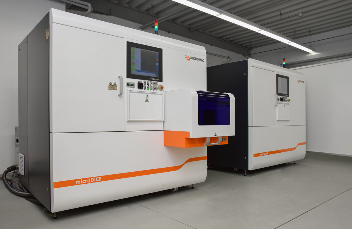
Then, in early 2014, Jenoptik's Lasers and Material Processing division sold its TLS-Dicing intellectual property to laser micromachining business, 3D-Micromac. Within months, 3D-Micromac had launched its microDICE laser dicing system, based on TLS-Dicing, designed for myriad brittle materials, but targetting SiC wafers for power device and LED applications.
According to Zuehlke, the latest system includes an array of software updates to enhance reproducibility, but fundamentally, it's based on the TLS two-step process.
Firstly, a short pulse ablation laser scribes a 10 micron-wide, 15 micron-deep line - dubbed the dicing street - to initiate a crack. Then, in the second step, a continuous wave laser is passed along this line to heat up the material locally to some 100°C; which is then rapidly cooled by spraying with distilled water, cleaving the wafer.
Crucially, as Zuehlke points out, the entire process takes place in a single pass. "This is very fast and entire wafer pieces are separated," he says. "Many other laser processes require many passes which reduces the throughput."
Indeed, trials reveal that fully processed 4H-SiC wafers, including the process control monitor (PCM) structures, backside metal layer stacks and the polyamide coating near to the dicing street, can be diced with feed rates as high as 200 mm/s. The temperature-sensitive polyamide coating is not affected, and as Zuehlke highlights, the resulting die is chip-free with smooth side-walls.
"Our industry partners tell me that for dicing SiC, standard mechanical sawing takes place at 4mm a second; any faster and the material gets too hot," he says. "But we run to 200mm a second, and this is the same for four and six inch wafers."

TLS-Dicing on a SiC wafer promises chip-free die separation.
But what about cost? 3D-Micromac's thermal laser separation tool is around three times more expensive than a mechanical sawing system. But given the tool's faster throughput, as well as reduced consumables, namely saw blades, Zuehlke reckons investment will break even within a few months.
"If you are dicing more than 150 wafers a month, our system will be less expensive than mechanical dicing, and that's including investment," he says.
So given the cost and throughput-benefits of thermal laser separation, Zuehlke is confident that the SiC market is ready for the technology. "Nearly all customers are using mechanical sawing at the moment and this is fine if you only have a small number of wafers," he says. "But given the volume increases predicted for SiC, we know customers are now looking for new dicing technologies."
Indeed, 3D-Micromac claims its dicing system is already being used by major industrial manufacturers for volume production for power devices.
"You can use [microDICE] on other material including silicon and sapphire but we will focus on SiC right now as the difference in cost of ownership is the most distinct," concludes Zuehlke.


