US team patents Cubic GaN approach

A team from the Center for Lighting Enabled Systems & Applications (LESA) faculty of Rensselaer Polytechnic Institute and the University of New Mexico (UNM) were recently awarded US Patent 9,520,472 for 'Growth of Cubic Crystalline Phase Structure on Silicon Substrates and Devices comprising the Cubic Crystalline Phase.'
This patent was issued on December 13, 2016 and included principal investigator Steven R. J. Brueck and inventors Sueng-Chang Lee (UNM), Christian Wetzel, Theeradetch Detchprohm (LESA/RPI), and Christoph Stark (LESA/RPI Graduate). Both universities are partners in LESA based at Rensselaer Polytechnic Institute in Troy, NY.
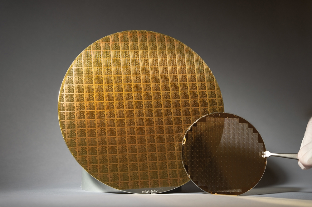
The patent describes a semiconductor device that includes a substrate comprising a groove, with a buffer layer formed on the groove surface. The buffer comprises at least one material chosen from AIN, GaN or Al.sub.xGa.sub.1-xN, where x is between zero and one. An epitaxially grown semiconductor material is disposed over the buffer layer, at least a portion of the epitaxially grown semiconductor material having a cubic crystalline phase structure.
Cubic GaN devices hold promise for addressing two long-standing issues that limit the performance of LEDs. Poor performance at longer emission wavelengths known as the green gap problem; and poor performance at higher operating current, known as efficiency droop.
GaN crystals can be grown with either cubic or hexagonal (also known as wurtzite) phases. All commercial GaN LEDs are based on hexagonal materials, typically grown on sapphire substrates.
"The hexagonal phase typically forms most easily, as it is the lowest energy crystallographic structure. Previous attempts to grow cubic GaN crystal structures have produced poor quality, heavily defected mixed phase materials ," said Christian Wetzel, Professor of Physics, Applied Physics and Astronomy, and co-inventor of this patent.
Wetzel and Brueck are both recognized leaders in the research and development of LED-based solid-state lighting.


