Loading...
News Article

Noel Technologies Expands Silicon Valley wafer fab

News

New lithography, deposition and measurement tools increase capacity and capabilities 


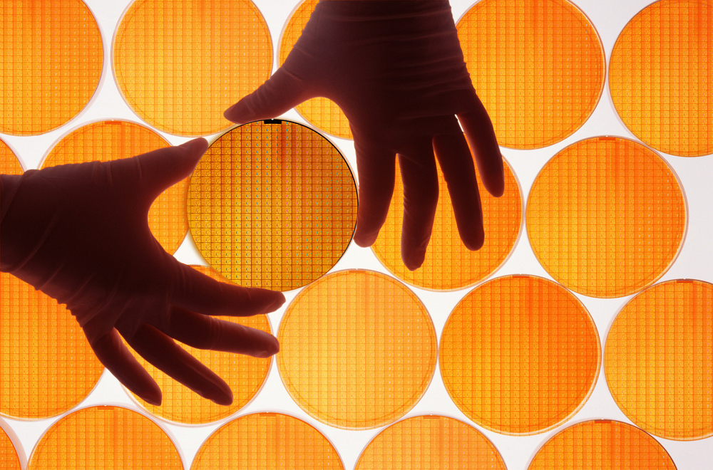
Noel Technologies, a specialty semiconductor foundry, has expanded its wafer-fabrication facility in Silicon Valley, California, by adding square footage and installing additional equipment that boost its production capacity by 25 percent.

With additions including an i-line lithography system with 0.35-micron resolution, a top-down CD scanning electron microscope (SEM) and more plasma-enhanced chemical vapor deposition (PECVD) tools, the 20-year-old company has increased its range of foundry services for customers in the semiconductor, MEMS, bio-medical device, sensor and LED markets.

"We perform many wafer-fabrication services integral to the development of the newest micro- and nanoelectronic products," said Leon Pearce, founder and chief technical officer of Noel Technologies. "As a manufacturing partner located right in Silicon Valley, we offer chip designers a local foundry solution to shorten their R&D cycles and reduce their time to production."

Noel Technologies specialises in helping chip designers that work with advanced non-CMOS materials and non-standard process flows. The company has decades of experience and proven capabilities in developing novel process flows involving III-V compound materials, gold, silver, transparent conductive oxides and emerging materials.

All front-end wafer processing is performed in-house under the supervision of Noel Technologies' process engineering team, eliminating the need for customers to coordinate work flows among multiple suppliers. The foundry's extensive process capabilities enable short manufacturing leadtimes while improving device yield and performance.

Say hello to the heterogeneous revolution
Double heterostructure HEMTs for handsets
AlixLabs to collaborate with Linköping University
SiC MOSFETs: Understanding the benefits of plasma nitridation
Wolfspeed reports Q2 results
VueReal secures $40.5m to scale MicroSolid printing
Mitsubishi joins Horizon Europe's FLAGCHIP project
Vishay launches new high voltage SiC diodes
UK team leads diamond-FET breakthrough
GaN adoption at tipping point, says Infineon
BluGlass files tuneable GaN laser patents
QD company Quantum Science expands into new facility
Innoscience files lawsuit against Infineon
Riber revenues up 5% to €41.2m
Forvia Hella to use CoolSiC for next generation charging
Photon Design to exhibit QD simulation tool
Ortel transfers CW laser fabrication to Canada
Luminus adds red and blue multi-mode Lasers
PseudolithIC raises $6M for heterogeneous chiplet tech
Mesa sidewall design improves HV DUV LEDs
IQE revenue to exceed expectations
'Game-changing' VCSEL system targets clinical imaging
German start-up secures finance for SiC processing tech
Macom signs preliminaries for CHIPS Act funding
IQE and Quintessent partner on QD lasers for AI
EU funds perovskite tandems for fuel-free space propulsion
EU to invest €3m in GeSi quantum project
Transforming the current density of AlN Schottky barrier diodes
Turbocharging the GaN MOSFET with a HfO₂ gate
Wolfspeed launches Gen 4 SiC MOSFET technology
Report predicts high growth for UK's North East
Element Six unveils Cu-diamond composite
×
Search the news archive

To close this popup you can press escape or click the close icon.
Logo
x
Logo
×
Register - Step 1

You may choose to subscribe to the Compound Semiconductor Magazine, the Compound Semiconductor Newsletter, or both. You may also request additional information if required, before submitting your application.


Please subscribe me to:


You chose the industry type of "Other"

Please enter the industry that you work in: