Loading...
News Article

Researchers achieve higher growth quality with GaN on SOI

News

Insulating layer in SOI wafers also improves breakdown characteristics for power electronics

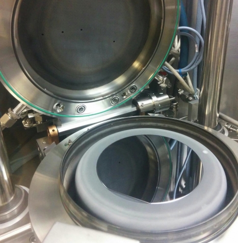
Working with Okmetic Oy and the Polish ITME, researchers at Aalto University in Finland have shown that SOI (Silicon On Insulator) wafers are suitable for growing GaN layers, reducing defects and strain compared to silicon substrates.

SOI wafers have a layer of silicon dioxide insulator sandwiched between two silicon layers in order to improve the capacitive and insulating characteristics of the wafer.

We used a standardised manufacturing process for comparing the wafer characteristics. GaN growth on SOI wafers produced a higher crystalline quality layer than on silicon wafers. In addition, the insulating layer in the SOI wafer improves breakdown characteristics, enabling the use of clearly higher voltages in power electronics. Similarly, in high frequency applications, the losses and crosstalk can be reduced", explains Jori Lemettinen, a doctoral candidate from the Department of Electronics and Nanoengineering.

GaN based components are becoming more common in power electronics and radio applications. The performance of GaN based devices can be improved by using a SOI wafer as the substrate", adds Academy Research Fellow Sami Suihkonen.

SOI wafers reduce the challenges of crystal growth

Growth of GaN on a silicon substrate is challenging because of the difference between the materials' coefficients of thermal expansion and lattice constants. These limit the crystalline quality that can be achieved and the maximum possible thickness of the produced layer.

"The research showed that the layered structure of an SOI wafer can act as a compliant substrate during GaN layer growth and thus reduce defects and strain in the grown layers", Lemettinen notes.

The work has been accepted for publication in the journal
Semiconductor Science and Technology


Say hello to the heterogeneous revolution
Double heterostructure HEMTs for handsets
AlixLabs to collaborate with Linköping University
SiC MOSFETs: Understanding the benefits of plasma nitridation
Wolfspeed reports Q2 results
VueReal secures $40.5m to scale MicroSolid printing
Mitsubishi joins Horizon Europe's FLAGCHIP project
Vishay launches new high voltage SiC diodes
UK team leads diamond-FET breakthrough
GaN adoption at tipping point, says Infineon
BluGlass files tuneable GaN laser patents
QD company Quantum Science expands into new facility
Innoscience files lawsuit against Infineon
Riber revenues up 5% to €41.2m
Forvia Hella to use CoolSiC for next generation charging
Photon Design to exhibit QD simulation tool
Ortel transfers CW laser fabrication to Canada
Luminus adds red and blue multi-mode Lasers
PseudolithIC raises $6M for heterogeneous chiplet tech
Mesa sidewall design improves HV DUV LEDs
IQE revenue to exceed expectations
'Game-changing' VCSEL system targets clinical imaging
German start-up secures finance for SiC processing tech
Macom signs preliminaries for CHIPS Act funding
IQE and Quintessent partner on QD lasers for AI
EU funds perovskite tandems for fuel-free space propulsion
EU to invest €3m in GeSi quantum project
Transforming the current density of AlN Schottky barrier diodes
Turbocharging the GaN MOSFET with a HfO₂ gate
Wolfspeed launches Gen 4 SiC MOSFET technology
Report predicts high growth for UK's North East
Element Six unveils Cu-diamond composite
×
Search the news archive

To close this popup you can press escape or click the close icon.
Logo
x
Logo
×
Register - Step 1

You may choose to subscribe to the Compound Semiconductor Magazine, the Compound Semiconductor Newsletter, or both. You may also request additional information if required, before submitting your application.


Please subscribe me to:


You chose the industry type of "Other"

Please enter the industry that you work in: