
Researchers simplify fabrication of nanowire UV-LEDs on silicon
KAUST team demonstrates dislocation-free AlGaN nanowires that spontaneously coalesce to allow device fabrication without planarisation
There is a growing demand for mercury-free, environmentally friendly, compact UV LEDs for disinfection applications. Existing AlGaN-based planar UVLEDs, however, suffer from high dislocation densities, low light extraction efficiency and poor p-doping efficiency, which limits the irmaximum output power to several mWs at 20 mA.
Dislocation-free AlGaN nanowires have shown better p-doping and light extraction efficiency but the growth of self-assembled, vertically oriented and uniform nanowires has remained a challenge. Furthermore, the nanowire-based LEDs require a planarisation process to first fill the gap between nanowires and then to make ohmic contacts. Planarisation is expensive and significantly reduces the light extraction efficiency due to the extreme absorption of the filling materials in the UV wavelengths.
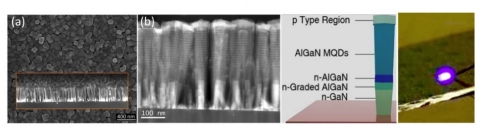
Now researchers at KAUST (King Abdullah University of Science and Technology), led by Bilal Janjua and Haiding Sun, have reported synthesising AlGaN nanowires that spontaneously coalesce with a high density of ~1 x 1010 cm-2 (filling factor >95 percent) using plasma-assisted MBE on silicon.
They say that their approach, published in the journal Nanoscale, offers a viable way to easily fabricate ultra-thin UV LEDs on low-cost and scalable silicon substrates, without the planarisation step.
In addition, they demonstrated AlGaN quantum disks (Qdisks are the nanowire equivalent of quantum wells) in the nanowires and showed segregation of Al/Ga locally within the Qdisk (nanoclusters) that enhanced luminescence, similar to that reported in InGaN-based quantum wells.
AlxGa1-xN /AlyGa1-yN multiple quantum-disks should have superior carrier confinement and thus improve the optical performance of the device. Device simulation results showed a large overlap of the electrons and holes wave functions in the active region because of the quantum confinement effect.
LEDs emitting at ~303 nm with a narrow FWHM (~20 nm) of the EL spectrum were demonstrated by using a large active region ("˜active region/nanowire length-ratio' ~ 50 percent) embedded with 15 stacks of AlxGa1-xN/AlyGa1-yN Qdisks.
According to the researchers, this is early work and more can be done to further improve the device performance. Nevertheless, they say their pendeo-epitaxy technique offers the possibility of simplifying the fabrication of a wide range of UV-nanowire devices such as lasers, photodetectors, modulators, and silicon integrated photonics.
"˜Self-planarized quantum-disks nanowires ultraviolet-B emitter utilizing pendeo-epitaxy' by Bilal Janjua et al, Nanoscale, 2017, DOI: 10.1039/C7NR00006E.


