Loading...
News Article

Soitec ramps SOI wafer production in China

News
Second source of 200mm SOI wafers enables Soitec to expand supply for growing market

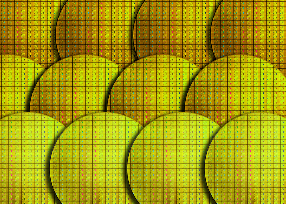
Soitec has announced that the ramp up to high-volume production of 200mm silicon-on-insulator (SOI) wafers - manufactured with Soitec's Smart Cut technology - has begun at the manufacturing facility of its Chinese partner Shanghai Simgui Technology fully qualified by key Soitec customers.

This successful implementation of a partnership model represents a key milestone for Soitec in managing its worldwide manufacturing capacity to meet market demand for 200mm SOI wafers used in fabricating semiconductors for the growing communications and power device markets.

"Establishing this second source in China allows us to ensure the needed capacity of 200mm SOI wafers from two sites in different regions of the world, with each facility producing exactly the same products from a specifications and quality standpoint," said Bernard Aspar, executive senior vice president of Soitec's Communication & Power Business Unit.

"Our partnership with Simgui is now running in an efficient way and our customers have been supportive and instrumental in this strategic move, which fully validates Soitec's technology-transfer expertise and manufacturing strategy."

"Simgui has been working on SOI materials for 16 years in China. Partnering with Soitec, Simgui is fully ready to support Soitec's ramp up of 200-mm SOI wafers manufactured with the Smart Cut technology at our facility in Shanghai and to help in developing the SOI ecosystem in China," said Jeffrey Wang, CEO of Simgui.

The first 200mm SOI wafers produced at Simgui's manufacturing facility in Shanghai using Soitec's proprietary Smart Cut technology were qualified by the initial customers at the end of last year.

Additional customers are currently in the process of qualifying the wafers. Producing the wafers in China has been a key objective of Soitec's and Simgui's licensing and technology-transfer agreement, signed in May 2014, and validates Smart Cut as a standard process. This wafer production line in China will boost the industrial manufacturing capacity of 200mm SOI wafers to meet increasing worldwide usage and also will be a key element in establishing the SOI ecosystem in China.

Soitec's 200mm RF-SOI and Power-SOI products are dedicated to the mobile and automotive markets respectively. As the leading SOI substrate innovator and manufacturer, Soitec has the largest worldwide capacity and produces both 200mm and 300mm wafers at multiple fabs in France.

Simgui will be exhibiting Soitec's Smart Cut-based 200mm product line at SEMICON China in Shanghai, March 14-16.

SPONSOR MESSAGE

Secure Your Hydrogen Supply

A study supply of high-purity hydrogen is critical to semiconductor fabrication. Supply chain interruptions are challenging manufacturers, leading to production slowdowns and stoppages. On-site hydrogen generation offers a scalable alternative for new and existing fabs, freeing the operator from dependence on delivered gas.

Plant managers understand the critical role that hydrogen plays in semiconductor fabrication. That important job includes crystal growth, carrier gas, wafer annealing, and in the emerging Extreme UV Lithography (EUV) that will enable new generations of devices. As the vast need for semiconductors grows across all sectors of world economies, so does the need for high-purity hydrogen.

Take control with Nel on-site hydrogen generation.

Read more
Say hello to the heterogeneous revolution
Double heterostructure HEMTs for handsets
AlixLabs to collaborate with Linköping University
SiC MOSFETs: Understanding the benefits of plasma nitridation
Wolfspeed reports Q2 results
VueReal secures $40.5m to scale MicroSolid printing
Mitsubishi joins Horizon Europe's FLAGCHIP project
Vishay launches new high voltage SiC diodes
UK team leads diamond-FET breakthrough
GaN adoption at tipping point, says Infineon
BluGlass files tuneable GaN laser patents
QD company Quantum Science expands into new facility
Innoscience files lawsuit against Infineon
Riber revenues up 5% to €41.2m
Forvia Hella to use CoolSiC for next generation charging
Photon Design to exhibit QD simulation tool
Ortel transfers CW laser fabrication to Canada
Luminus adds red and blue multi-mode Lasers
PseudolithIC raises $6M for heterogeneous chiplet tech
Mesa sidewall design improves HV DUV LEDs
IQE revenue to exceed expectations
'Game-changing' VCSEL system targets clinical imaging
German start-up secures finance for SiC processing tech
Macom signs preliminaries for CHIPS Act funding
IQE and Quintessent partner on QD lasers for AI
EU funds perovskite tandems for fuel-free space propulsion
EU to invest €3m in GeSi quantum project
Transforming the current density of AlN Schottky barrier diodes
Turbocharging the GaN MOSFET with a HfO₂ gate
Wolfspeed launches Gen 4 SiC MOSFET technology
Report predicts high growth for UK's North East
Element Six unveils Cu-diamond composite
×
Search the news archive

To close this popup you can press escape or click the close icon.
Logo
x
Logo
×
Register - Step 1

You may choose to subscribe to the Compound Semiconductor Magazine, the Compound Semiconductor Newsletter, or both. You may also request additional information if required, before submitting your application.


Please subscribe me to:


You chose the industry type of "Other"

Please enter the industry that you work in:
 
x
Adblocker Detected
Please consider unblocking adverts on this website