Green light for GaN devices

Exagan and X-Fab prepare for mass production after delivering GaN-on-silicon devices on a 200 mm CMOS process, reports Rebecca Pool.
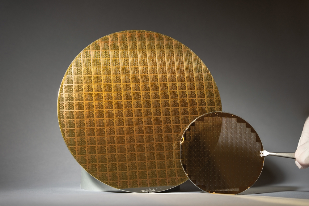
X-Fab and Exagan are producing GaN-on-silicon devices in a CMOS fab.
In a breakthrough for GaN-on-silicon device markets, industry partners, X-Fab and Exagan, have produced transistors on a 200 mm, CMOS process.
With substrate fabrication taking place at Exagan's 200 mm epi-manufacturing facility in Grenoble, France, followed by device processing at X-Fab's CMOS foundry in Dresden, Germany, prototype 650 V G-FETs are currently with first customers.
Crucially, plans to ramp production are underway with mass production well within the companies' sights.
"We are the first to transfer and produce devices on 200 mm wafers, with manufacturing quality, in a CMOS fab using standard silicon production equipments and process steps," highlights Frédéric Dupont, president and chief executive at Exagan. "Importantly, we have established our technology and products on the most competitive wafer size; taking advantage of the mature, 200 mm, and highly productive, manufacturing environment."
"Once our product is established on the market, we will be able to work with X-Fab to ramp up capacity very quickly," he adds.
Exagan's GaN-on-silicon technology has been under development since the late 1990s.
Researchers at France-based hetero-epitaxy research centre, CNRS-CRHEA spent more than a decade grappling with the different thermal coefficients of silicon and GaN that cause materials stresses, and ultimately cracking, when a GaN film is grown on silicon.
But come 2003, a GaN-buffer - for the growth of thick, high quality GaN layers on silicon - had been developed and patented by wide bandgap semiconductor business, Picogiga, France, later acquired by semiconductor material manufacturer, Soitec, also of France.
In 2012, Soitec joined forces with electronics research institute, CEA-Leti, France, to develop a 200 mm, CMOS-compatible GaN-based FET process for 650 V power switching devices with the technology then being transferred to Exagan for commercialisation.
Collaboration with X-Fab began in 2015 and in just two years, several barriers to 200 mm CMOS process success have been overcome.
![]() Frédéric Dupont, President, CEO and Co-Founder of Exagan (right) and X-Fab Chief Technology Officer, Jens Kosch.
Frédéric Dupont, President, CEO and Co-Founder of Exagan (right) and X-Fab Chief Technology Officer, Jens Kosch.
Importantly, says Dupont, Exagan has developed its so-called G-Stack material technology, based on the CNRS-CRHEA buffer layer and including GaN insulating layers and strain management layers. These layers relax the GaN crystal stresses, improving crystal quality and yielding crack-free, flat wafers for CMOS manufacture.
"The larger the diameter, the more challenging it is to get a perfectly flat wafer, and managing cracks and bowing has been a huge challenge," he says. "But G-Stack has addressed this and we can manufacture wafers that are fully compliant with the CMOS process."
Indeed, as Dupont's colleague and X-Fab chief technology officer, Jens Kosch, points out, the additional buffer layers usually require increased wafer thickness, and could have presented a problem for CMOS production.
As he says: "It was a real challenge to get the necessary wafer bow for the CMOS process while retaining an acceptable silicon wafer thickness, but we have achieved this and resolved equipment compatibility problems."
The GaN-on-silicon fabrication process adheres to the strict contamination rules of a standard CMOS process. "We also use fully-automated, epitaxy equipment for our eight inch process - including automated wafer handling - to avoid any contact and wafer contamination," says Dupont.
Crucially, not a single, additional processing step or tool is required to support GaN-on-silicon device fabrication. "We really wanted full compatibility with the CMOS line, with no extra process steps of specific tools," highlights Kosch. "Our common goal from day one was to avoid additional capital expenditure and we can now use a standard CMOS manufacturing line, running at volume production levels, for this new GaN material."
Right now, Exagan is sampling 650 V G-FETs to its first customers. Devices have been described as having a high breakdown voltage, low vertical leakage and high operating temperature, although according to Dupont, specific performance figures cannot yet be revealed.
Exagan has also been working with Germany's certification services business, TÜV Nord, to achieve product qualification meeting automotive and aerospace industry standards.
Electric vehicle charging will be amongst the initial targeted applications for Exagan's 650 V G-FETs; a growing market already under scrutiny from the likes of Fujitsu, Infineon and other SiC and GaN suppliers.
"There are many companies working on GaN but our technology and business model are unique; we control the full technology flow from the epitaxy to system level," asserts Dupont.
"Critically, our partnership with X-Fab gives us the capacity to ramp very quickly to high volumes and with very cost competitive devices," he adds. "I believe we will soon be recognised as the GaN market accelerator."


