WIN Semiconductors Develops GaAs PIN Diode MMIC Process

Flexible process targets high frequency switch and limiter applications
Taiwanese compound semiconductor foundry WIN Semiconductors has developed an advanced GaAs PIN diode MMIC process for high frequency switch and monolithic power limiter applications.
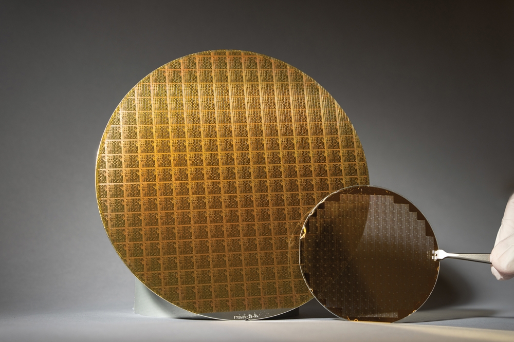
Fabricated on 150mm semi-insulating GaAs wafers, the 3µm i-layer PIN diodes is said tooffer several performance advantages including near constant junction capacitance through 50 GHz, low insertion loss, and excellent isolation required for high frequency applications.
The PIN3-00 GaAs PIN diode MMIC process uses a humidity robust architecture with low-k dielectric crossovers, and three interconnect metal layers with up to 7µm thick Au metallisation for high Q-factor passive elements.
"This advanced PIN diode MMIC fabrication process offers significant design flexibility for multiple applications and end-markets. The PIN3-00 process can be used for receive path limiters in Radar Tx/Rx modules, power switching as well as high frequency 5G switch functions.
WIN is the first compound semiconductor foundry to offer this high performance technology on 150mm wafers, and at the scale required for high volume markets" said David Danzilio, senior VP of WIN Semiconductors.


