
Zeiss Enters Semiconductor Process Control Market
Zeiss is expanding into the semiconductor industry. Its new Process Control Solutions (PCS) business unit will draw on long standing innovations in microscopy that Zeiss is well known for.
The newly opened Zeiss Customer Centre located near the heart of Silicon Valley in Pleasanton, California, will offer demonstrations, applications development and training on the company's portfolio of optical, ion, electron and X-ray microscopy offerings, including process control solutions.
"We see a strong trend in semiconductors toward complex 3D chip structures and new materials," explained Karl Lamprecht, head of SMT business group. "As development cycles lengthen and R&D costs climb, the role of metrology changes. Our customers need effective process control solutions delivering integrated, actionable information that speeds time to problem resolution and time to production. Zeiss has the technology and expertise to fulfill these requirements."
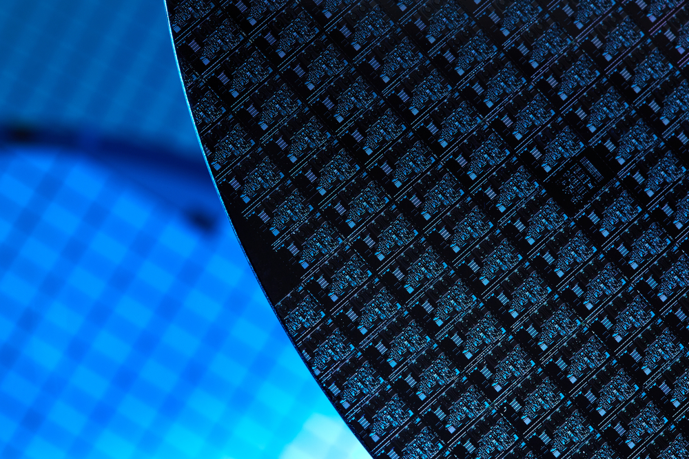
With shrinking structure sizes, ever more sophisticated designs and hundreds of individual working steps, the semiconductor manufacturing workflow has become increasingly challenging. Fast and cost-effective process control solutions play a key role in ensuring the functioning of semiconductor devices. Zeiss already has a portfolio of lithography optics and mask metrology and repair solutions, and is now bringing its semiconductor equipment experience into the market for semiconductor process control solutions.
The PCS business unit will use and expand upon Zeiss's existing portfolio of products, including its core proprietary microscopy technologies, to penetrate the semiconductor lab and fab space.
Key products to be deployed include Zeiss's electron microscope products Zeiss Crossbeam and Zeiss MultiSEM (the latter of which incorporates the company's unique multi-electron-beam technology), ion-beam microscope Zeiss ORION NanoFab, as well as the Zeiss Xradia Versa and Zeiss Xradia Ultra non-destructive 3D X-ray microscope systems.
Process control solutions will be offered across the spectrum of semiconductor manufacturing process steps, including front end of line (FEOL), back end of line (BEOL), packaging and assembly.
"Our process control solutions offer comprehensive structural, chemical and electrical information. By creating a single window into Zeiss for our semiconductor customers, we will enable them to address their process control challenges with seamlessly integrated technologies, helping them get their products to market faster," said Raj Jammy, head of Zeiss PCS business unit, headquartered in Pleasanton, California.
Jammy, who has more than 20 years of extensive semiconductor industry experience, joined Zeiss in February 2016. After obtaining a Ph.D. in electrical engineering from Northwestern University, he started his career at IBM in New York and held subsequent leading positions at SEMATECH and Intermolecular. Jammy and his team will collaborate closely with global customers to address semiconductor inspection and review, failure analysis, defect detection, 3D tomography, and process characterisation and analysis.
Zeiss will showcase its latest microscopy products and solutions for semiconductor manufacturing at SEMICON West, to be held July 11-13 at the Moscone Convention Center in San Francisco, California.


