Ultraviolet LEDs take aim at disinfection

As Osram Opto pours more resources into deep UV LEDs, are the devices nearing commercialisation, asks Rebecca Pool.
While long-wavelength, ultraviolet LEDs have swiftly penetrated curing applications worldwide, shorter wavelength deep UV LEDs, designed for disinfection, have faltered.
UV-A LEDs, emitting at 315 to 400 nm, are fabricated by growing InGaN-based epilayers on sapphire substrates via the tried-and tested MOCVD methods used in visible LED markets. But the deep UV LED is different.
Emitting at 200 to 280 nm, many of these UV-C LEDs comprise AlN layers on a sapphire wafer, with ensuing strain-related epitaxy issues stymieing manufacturing progress. But change is afoot.
As UV LEDs markets have gathered momentum, AlN substrate manufacturers such as CrystAL-N, Germany, Crystal IS and Hexatech, both of the US, have been quick to ensure native, lattice-matched wafers are ready to take on the readily available sapphire rival. And device manufacturers are biting.
Earlier this year, Germany-based Osram Opto Semiconductors signed a long-term licensing deal with US-based Hexatech to accelerate UV-C LED device development based on HexaTech's material. And just recently the LED manufacturer revealed it was leading a project - UNIQUE - to develop and commercialise high power AlGaN-on-AlN UV LEDs for industrial disinfection processes.
Supported by the Bavarian Ministry for Economic Affairs, Media, Energy and Technology, Osram Opto is joined by five Germany-based partners, and will establish the necessary supply chain to produce these LEDs. Osram Opto already has many of the necessary processes at its Regensburg site, thanks to the visible LED and laser volume production that takes place here, but the project will provide much more.
Aprotec is set to manufacture the crystal growth furnace while the Fraunhofer Institute for Integrated Systems and Device Technology will coordinate AlN crystal growth processes.
Osram Opto itself will develop the UVC LED chip and associated epitaxy and processing, Schott is to develop the much-needed vacuum-tight packaging, and UV LED system developer, Dr Hönle AG, will integrate the LED modules to the disinfection system.
As Hans-Juergen Lugauer, Head of UV-LED Research and Development at OSRAM Opto, asserts: "From AlN substrate production and chip fabrication to packaging and the final product for the end user, we will establish the complete value chain necessary for deep UV LEDs and related products in Bavaria."
Lugauer doesn't anticipate that AlN wafers will be available in the necessary volumes for volume production as the project closes, but as he puts it: "The Hexatech agreement was an independent move to secure access to high quality AlN wafers as soon as possible."
Wafer dilemma
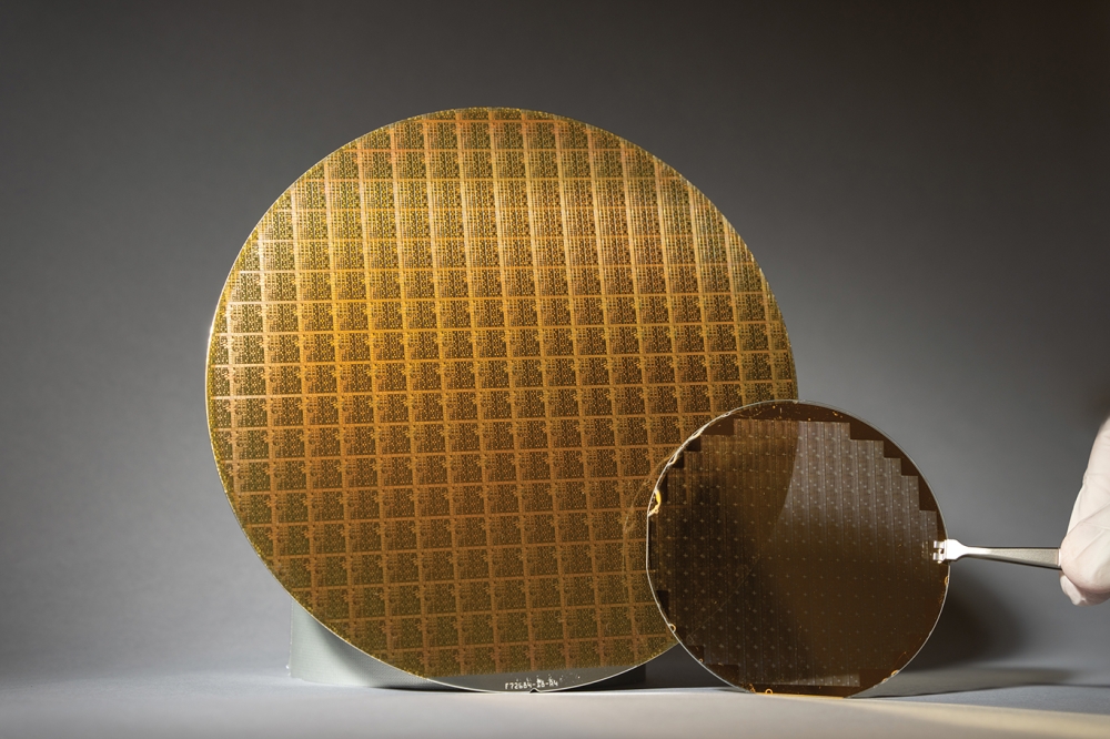
Right now, Osram Opto is using two inch sapphire wafers for UV LED epitaxy and chip development, implementing a AlN buffer layer to manage lattice strains. However, researchers at the company have already been busy experimenting with epitaxy on AlN substrates, and work will continue as part of the UNIQUE project.
"We've been performing the epitaxy experiments in parallel, to be ready to transfer all processes to two inch wafer as soon as they are available in quantities," highlights Lugauer.
As part of its work, Osram Opto is using MOVPE growth to fabricate AlGaN thin films for deep UV LEDs. As Lugauer points out, dislocation densities on AlN/sapphire templates are currently around 109/cm2 but drop to less than 104/cm2 structures on AlN substrates.
"It is not yet clear whether the dislocation densities on AlN/sapphire templates are low enough to achieve the high efficiency and reliability needed for high current density disinfection applications," says Lugauer.
And as the head of UV-LED R&D points out, the efficiency of AlGaN-based structures is very sensitive to defects and dislocations. He questions whether or not even shorter wavelength applications, such as gas sensing, would be able to use sapphire substrates at all.
"The AlN substrates offer a very low dislocation density, which should have a positive effect on device efficiency and lifetime, and provide us with the high performance, high quality devices Osram Opto is known for," he adds.
Lugauer also highlights how using the native AlN substrates with AlGaN layers reduces thermally induced stresses and wafer bow after epitaxy. "The large bow of deep UV LEDs on sapphire sometimes completely prevents automated wafer handling in our chip processing line but [using AlN wafers] eases wafer handling," he says.
"The bow issue increases significantly as wafers scale up in size, which currently makes the use of four and six inch sapphire substrates more or less impossible for deep UV LEDs processing," he adds. "In contrast, as soon as larger AlN substrates are available, the processes can be straightforwardly transferred to the [bigger] size."
Still, Lugauer admits sapphire substrates are a lot cheaper, so Osram Opto will be pursing both substrate routes until the materials advantages and limits are clearer. "Then we will decide on the most practical approach," he says. "It might turn out that we will use both substrates to cover different application requirements."
In the meantime, Lugauer has his eyes firmly fixed on the epitaxy and chip processes. He believes the key steps to cost effective volume production of deep UV LEDs are to develop an epitaxy process that yields LEDs with a high internal quantum efficiency as well as a chip process that produces devices with high current stability and light extraction to deliver an external quantum efficiency of more than 10%.
"Both of these processes are now being developed within our project, but we don't expect production to be ready before 2020," he says.


