Loading...
News Article

Monocrystal delivers 150-millionth two inch equivalent wafer

News

Russian sapphire firm estimates that every third LED and every tenth solar module is made with its products

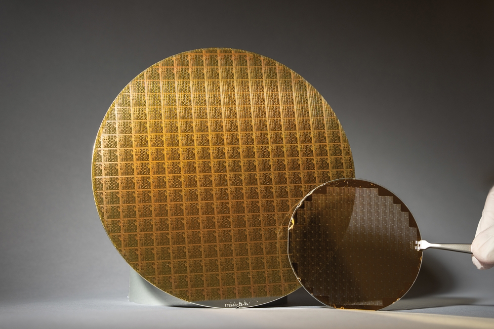
Monocrystal, a Russian maker of synthetic sapphire growing and processing, has announced the shipment of its 150-millionth two-inch equivalent (TIE) product.

Since its incorporation in 1999, the company has transformed from a niche sapphire market player into a well-established high-volume manufacturer. According to the company's estimates, every third LED and every tenth solar module in the world is made with Monocrystal products.

"Historically more than 60 percent out of 150 million TIE have been large diameter wafers and ingots for LED. We are now seeing an increasing demand for our 6-inch wafers since major LED manufacturers prefer our product due to its impeccable performance during nitride growth," said Monocrystal's CEO Oleg Kachalov.

"Monocrystal's low stress wafers demonstrate low thermal bow in the epitaxial process. As a result, our customers get tighter wavelength uniformity and increase their binning yields by 2-3 percent, which is significant for high volume production. 6-inch wafers are yet to become the driver of efficiency improvement, while Monocrystal's customers are already enjoying the benefits of stable yields and lower costs."

VP marketing Ludmila Zubova added: "The LED industry has made significant progress over the past few years but still there are future opportunities. For instance, microLEDs seem to be a feasible and promising technology. Monocrystal has already delivered ultra-clean wafers for this application. We have several initiatives running to support customers engaged in microLED development."

Say hello to the heterogeneous revolution
Double heterostructure HEMTs for handsets
AlixLabs to collaborate with Linköping University
SiC MOSFETs: Understanding the benefits of plasma nitridation
Wolfspeed reports Q2 results
VueReal secures $40.5m to scale MicroSolid printing
Mitsubishi joins Horizon Europe's FLAGCHIP project
Vishay launches new high voltage SiC diodes
UK team leads diamond-FET breakthrough
GaN adoption at tipping point, says Infineon
BluGlass files tuneable GaN laser patents
QD company Quantum Science expands into new facility
Innoscience files lawsuit against Infineon
Riber revenues up 5% to €41.2m
Forvia Hella to use CoolSiC for next generation charging
Photon Design to exhibit QD simulation tool
Ortel transfers CW laser fabrication to Canada
Luminus adds red and blue multi-mode Lasers
PseudolithIC raises $6M for heterogeneous chiplet tech
Mesa sidewall design improves HV DUV LEDs
IQE revenue to exceed expectations
'Game-changing' VCSEL system targets clinical imaging
German start-up secures finance for SiC processing tech
Macom signs preliminaries for CHIPS Act funding
IQE and Quintessent partner on QD lasers for AI
EU funds perovskite tandems for fuel-free space propulsion
EU to invest €3m in GeSi quantum project
Transforming the current density of AlN Schottky barrier diodes
Turbocharging the GaN MOSFET with a HfO₂ gate
Wolfspeed launches Gen 4 SiC MOSFET technology
Report predicts high growth for UK's North East
Element Six unveils Cu-diamond composite
×
Search the news archive

To close this popup you can press escape or click the close icon.
Logo
x
Logo
×
Register - Step 1

You may choose to subscribe to the Compound Semiconductor Magazine, the Compound Semiconductor Newsletter, or both. You may also request additional information if required, before submitting your application.


Please subscribe me to:


You chose the industry type of "Other"

Please enter the industry that you work in: