
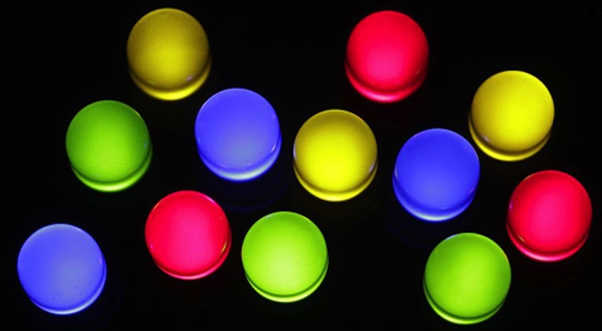
Researchers tune perovskite LED wavelengths
German team uses waffle patterned wafer to tune size of semiconducting nanocrystals based on perovskite
Researchers at the Ludwig-Maximilians-Universitaet (LMU) in Munich have found a clever and economical way of tuning the colour of the light emitted by an LED by altering the size of their semiconductor crystals.
The exact wavelength of light emitted from LEDs is determined by the chemical composition of the semiconductor employed. In the case of some semiconducting materials, the colour can also be tuned by modifying the size of the crystals of which the light-emitting layer is composed. In crystals with dimensions on the order of a few nanometers, quantum mechanical effects begin to make themselves felt.
LMU researchers in collaboration with colleagues at the University of Linz (Austria) have now developed a method for the production of semiconducting nanocrystals of defined size based on the cheap mineral oxide perovskite. These crystals are extremely stable, which ensures that the LEDs exhibit high colour fidelity - an important criterion of quality. Moreover, the resulting semiconductors can be printed on suitable surfaces, and are thus suitable for the manufacture of LEDs for use in displays.
The crucial element in the new method is a thin wafer, only a few nanometers thick, which is patterned like a waffle. The depressions serve as tiny reaction vessels, whose shape and volume ultimately determine the final size of the nanocrystals. "Optimal measurements of the size of the crystals were obtained using a fine beam of high-energy X-radiation at the Deutsche Elektronen-Synchrotron (DESY) in Hamburg", says LMU researcher Bert Nickel, member of the Nanosystems Initiative Munich (NIM), a Cluster of Excellence.
Moreover, the wafers are produced by means of an economical electrochemical process, and can be fashioned directly into LEDs. "Our nanostructure oxide layers also prevent contact between the semiconductor crystals and deleterious environmental factors such as free oxygen and water, which would otherwise limit the working lifetime of the LEDs," as Martin Kaltenbrunner of the Johannes Kepler University in Linz explains. In the next step, we want to enhance the efficiency of these diodes further, and explore their potential for use in other applications, such as flexible displays.
'Confining metal-halide perovskites in nanoporous thin films' by Stepan Demchyshyn et al; Science Advances 04 Aug 2017:Vol. 3, no. 8


