Loading...
News Article

New German research centre will focus on Graphene and 2D Materials
News

Aachen-based centre to bridge gap between science and applications within 2D materials based electronics and photonics

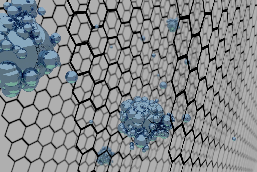
RWTH Aachen University and AMO GmbH, both partners in the EU Graphene Flagship, have launched a new joint research centre in Aachen, Germany. The aim is to bridge the gap between fundamental science and applications within graphene and related 2D materials based electronics and photonics.

The five founding Principal Investigators of the Aachen Graphene & 2D-Materials Centre are all members of the Graphene Flagship and share the vision of bringing graphene and related materials research from the lab into applications. "The Centre will help to turn the exciting properties of graphene and 2D-materials into true functions, making these materials not only fascinating for scientists but also serving society", Christoph Stampfer explains.

"With the Aachen Graphene & 2D-Material Centre, we aim at increasing the visibility of Aachen as an excellent place to undertake graphene and 2D material research with both a fundamental and applied focus."

The centre enables the integration of the already ongoing work from RWTH Aachen University and AMO GmbH under a legal framework that allows for full collaboration between the groups. In particular, the centre will focus on addressing the challenges of future technology including high-frequency electronics, flexible electronics, energy-efficient sensing, photonics as well as spintronics and valleytronics with graphene and related materials and their heterostructures.

The founding members of the Aachen Graphene & 2D-Materials Centre are Christoph Stampfer (RWTH and spokesman of the centre), Max Lemme (AMO and RWTH), Markus Morgenstern (RWTH), Renato Negra (RWTH) and Daniel Neumaier (AMO).

Say hello to the heterogeneous revolution
Double heterostructure HEMTs for handsets
AlixLabs to collaborate with Linköping University
SiC MOSFETs: Understanding the benefits of plasma nitridation
Wolfspeed reports Q2 results
VueReal secures $40.5m to scale MicroSolid printing
Mitsubishi joins Horizon Europe's FLAGCHIP project
Vishay launches new high voltage SiC diodes
UK team leads diamond-FET breakthrough
GaN adoption at tipping point, says Infineon
BluGlass files tuneable GaN laser patents
QD company Quantum Science expands into new facility
Innoscience files lawsuit against Infineon
Riber revenues up 5% to €41.2m
Forvia Hella to use CoolSiC for next generation charging
Photon Design to exhibit QD simulation tool
Ortel transfers CW laser fabrication to Canada
Luminus adds red and blue multi-mode Lasers
PseudolithIC raises $6M for heterogeneous chiplet tech
Mesa sidewall design improves HV DUV LEDs
IQE revenue to exceed expectations
'Game-changing' VCSEL system targets clinical imaging
German start-up secures finance for SiC processing tech
Macom signs preliminaries for CHIPS Act funding
IQE and Quintessent partner on QD lasers for AI
EU funds perovskite tandems for fuel-free space propulsion
EU to invest €3m in GeSi quantum project
Transforming the current density of AlN Schottky barrier diodes
Turbocharging the GaN MOSFET with a HfO₂ gate
Wolfspeed launches Gen 4 SiC MOSFET technology
Report predicts high growth for UK's North East
Element Six unveils Cu-diamond composite
×
Search the news archive

To close this popup you can press escape or click the close icon.
Logo
x
Logo
×
Register - Step 1

You may choose to subscribe to the Compound Semiconductor Magazine, the Compound Semiconductor Newsletter, or both. You may also request additional information if required, before submitting your application.


Please subscribe me to:


You chose the industry type of "Other"

Please enter the industry that you work in: