
OIST scientists improve perovskite solar cells and LEDs
Researchers increase solar cell lifetime by adding polymer layer and produce first perovskite LED using chemical vapour deposition
Researchers from the Okinawa Institute of Science and Technology (OIST) in Japan, have published two new scientific publications focusing on the improvement of perovskite solar cells and a cheaper and smarter way to produce emerging perovskite-based LED lights.
Perovskite structures are still plagued by a short lifespans due to stability issues. OIST scientists have made constant baby steps in improving the cells stability, identifying the degradations factors and providing solutions towards better solar cell architecture.
The new finding, reported in the Journal of Physical Chemistry B, suggests interactions between components of the solar cell itself are responsible for the rapid degradation of the device.
More precisely, the titanium oxide layer extracting electrons made available through solar energy "“ effectively creating an electric current "“ causes unwanted deterioration of the neighbouring perovskite layer.
The OIST researchers haveinserted in the solar cell an additional layer made from a polymer to prevent direct contact between the titanium oxide and the perovskite layers. This polymer layer is insulating but very thin, which means it lets the electron current tunnel through yet does not diminish the overall efficiency of the solar cell, while efficiently protecting the perovskite structure.
"We added a very thin sheet, only a few nanometers wide, of polystyrene between the perovskite layer and the titanium oxide layer," explained Longbin Qiu. "Electrons can still tunnel cross this new layer and it does not affect the light absorption of the cell. This way, we were able to extend the lifetime of the cell four-fold without loss in energy conversion efficiency".
The lifespan of the new perovskite device was extended to over 250 hours - still not enough to compete with commercial photovoltaic cells regarding stability, but an important step forward toward fully functional perovskite solar cells.
Manufacturing LEDs using CVD
The bipolar electronic properties of the perovskite structure not only confer them the ability to generate electricity from solar energy but also can convert electricity into vivid light.
Perovskite LEDs are envisaged to become the new industry standard in the near future due to the lower cost and their efficiency to convert power into light. Moreover, by changing the atomic composition in the perovskite structure, perovskite LED can be easily tuned to emit specific colours.
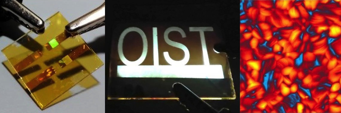
Manufacturing perovskite LEDs is currently based on dipping or covering the targeted surface with liquid chemicals, a process which is difficult to setup, limited to small areas and with low consistency between samples. To overcome this issue, OIST researchers, in collaboration with Chihaya Adachi and Chuanjiang Qin from Kyushu University, reported in the Journal of Physical Chemistry Letters the first perovskite LED assembled with CVD (pictured above).
"Chemical vapour deposition is already compatible with the industry, so in principle it would be easy to use this technology to produce LEDs," commented Yabing Qi. "The second advantage in using CVD is a much lower variation from batch to batch compared to liquid-based techniques. Finally, the last point is scalability: CVD can achieve a uniform surface over very large areas".
Like the solar cell, the perovskite LED also comprises many layers working in synergy. First, an indium tin oxide glass sheet and a polymer layer allow electrons into the LED. The chemicals required for the perovskite layer "“ lead bromide and methylammonium bromide - are then successively bound to the sample using CVD, in which the sample is exposed to gasses in order to convert to perovskite instead of typically solution-coating processes with liquid.
In this process, the perovskite layer is composed of nanometer-small grains, whose sizes play a critical role in the efficiency of the device. Finally, the last step involves the deposition of two additional layers and a gold electrode, forming a complete LED structure. The LED can even form specific patterns using lithography during the manufacturing process.
"With large grains, the surface of the LED is rough and less efficient in emitting light. The smaller the grain size, the higher the efficiency and the brighter the light," explained Lingqiang Meng. "By changing the assembly temperature, we can now control the growth process and the size of the grains for the best efficiency".
Controlling the grain size is not the only challenge for this first-of-its-kind assembling technique of LED lights. "Perovskite is great, but the choice in the adjacent layers is really important too," added Luis K. Ono. "To achieve high electricity-to-light conversion rates, every layer should be working in harmony with the others."
The result is a flexible, thick film-like LED with a customisable pattern. The luminance, or brightness, currently reaches 560 cd/m2, while a typical computer screen emits 100 to 1000 cd/m2 and a ceiling fluorescent tube around 12,000 cd/m2.
"Our next step is to improve the luminance a thousand-fold or more," concluded Meng. "In addition, we have achieved a CVD-based LED emitting green light but we are now trying to repeat the process with different combinations of perovskite to obtain a vivid blue or red light".


