GaN "˜Tangos' with Silicon to Overcome Material Limitations

UC San Diego team grow crack-free 19-micron-thick layers of GaN on silicon
Researchers at the Integrated Electronics and Biointerfaces Group at UC San Diego led by electrical engineering professor Shadi Dayeh have solved a classical problem of thermal mismatch when growing GaN on foreign substrates.
The origin of the problem is well known: high quality material deposition is usually carried out near 1,000degC, but when dissimilar materials are cooled down to room temperature, their contraction can be disproportionate, resulting in the formation of cracks and material failure.
Because the crack severity depends on the thickness of the layers, the thickest pure and semiconducting GaN layer that can be grown on silicon is 4.5µm thick - too thin to provide good use of GaN for high power (kilovolt-scale) applications which require much thicker layers (10 microns or more).
In an article published on Aug. 21 in Advanced Materials, the San Diego team combined fundamental crystal properties of GaN and geometrical effects to deflect strain from the crystal planes that usually crack under stress to the surface facets that can freely expand and contract in response to stress.
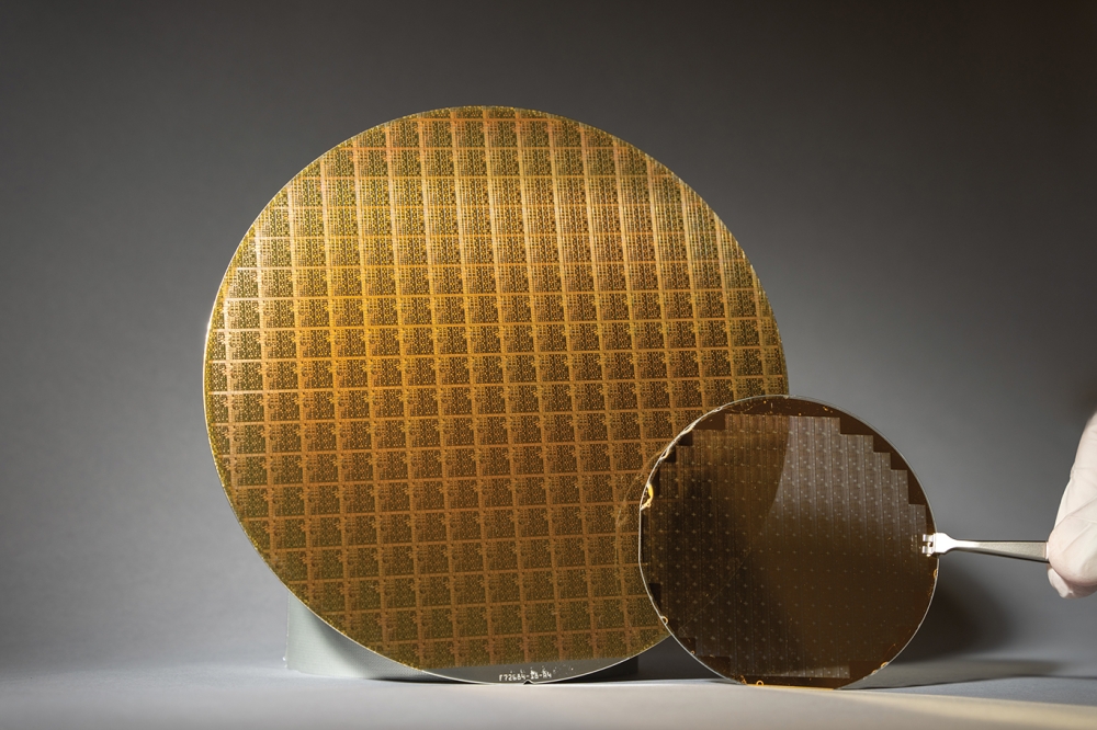
By doing so, they were able to grow crack-free 19-micron-thick layers of GaN on Si "” thicker than what's needed for high-power applications. In the resulting structures, both GaN and Si had exposed surfaces to enable them to move, twist or 'tango' together without cracking despite their thermal mismatch.
Thick layers also allowed the crystal defects "” threading dislocations "” to reduce from commonly achieved 108 "“ 109 per cm2 on Si to 107. And with the high material quality, Dayeh and his team demonstrated the first vertical GaN switches on silicon.
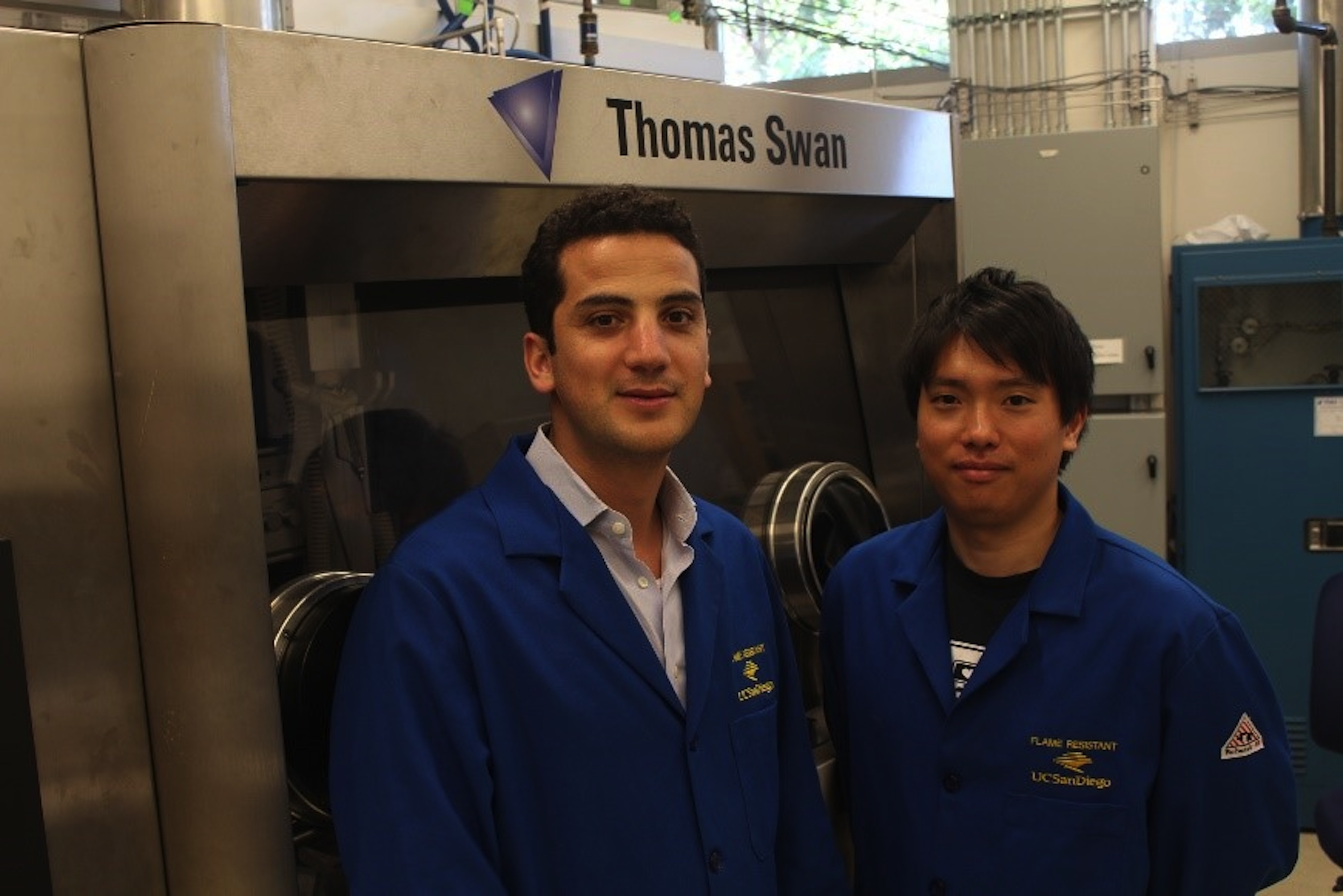
"This is the result of nearly four years of diligent efforts by graduate student Atsunori Tanaka, who learned and quickly excelled in the GaN MOCVD here at UC San Diego," said Dayeh. "A group of very talented students including Atsunori Tanaka, Woojin Choi, who fabricated the vertical switches, and Renjie Chen, who did the electron microscopy, have teamed up to complete the research," Dayeh continued. Based on this work, Dayeh received funding in July from the National Science Foundation to realise a monolithically integrated GaN power converter on Si.
The growth, device fabrication and characterisation were performed at UC San Diego and the electron microscopy was performed at the Center for Integrated Nanotechnologies (CINT), a Department of Energy Office of Basic Science user facility that provides access to top-of-the-line equipment under a user proposal system.


