
US team measures MoS2 band gap
Precise band gap measurement is 30 percent higher than expected
A team at the Department of Energy's Lawrence Berkeley National Laboratory has precisely measured the band gap of MoS2, a 2D semiconducting material. The team also revealed a powerful tuning mechanism and an interrelationship between its electronic and optical properties.
As reported in the Aug. 25 issue of Physical Review Letters, the researchers found that the band gap for a monolayer of MoS2, which has proved difficult to accurately predict theoretically, was 30 percent higher than expected based on previous experiments. They also quantified how the band gap changes with electron density - a phenomenon known as 'band gap renormalisation'.
"The most critical significance of this work was in finding the band gap," said Kaiyuan Yao, a graduate student researcher at Berkeley Lab and the University of California, Berkeley, who served as the lead author of the research paper.
"That provides very important guidance to all of the optoelectronic device engineers. They need to know what the band gap is" in orderly to properly connect the 2-D material with other materials and components in a device, Yao said.
Obtaining the direct band gap measurement is challenged by the so-called 'exciton effect' in 2D materials that is produced by a strong pairing between electrons and holes. The strength of this effect can mask measurements of the band gap.
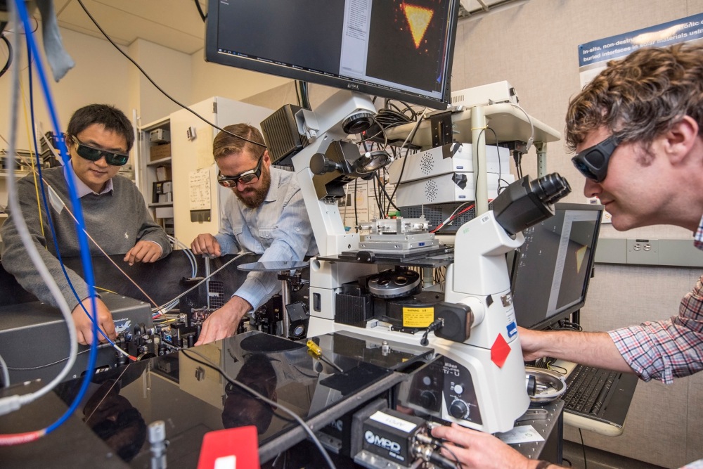
Nicholas Borys, a project scientist at Berkeley Lab's Molecular Foundry who also participated in the study, said the study also resolves how to tune optical and electronic properties in a 2D material."The real power of our technique, and an important milestone for the physics community, is to discern between these optical and electronic properties," Borys said. The team used several tools at the Molecular Foundry, a facility that is open to the scientific community and specialises in the creation and exploration of nanoscale materials.
The Molecular Foundry technique that researchers adapted for use in studying monolayer MoS2, known as photoluminescence excitation (PLE) spectroscopy, promises to bring new applications for the material within reach, such as ultrasensitive biosensors and tinier transistors, and also shows promise for similarly pinpointing and manipulating properties in other 2-D materials, researchers said.
The research team measured both the exciton and band gap signals, and then detangled these separate signals. Scientists observed how light was absorbed by electrons in the MoS2 sample as they adjusted the density of electrons crammed into the sample by changing the electrical voltage on a layer of charged silicon that sat below the MoS2 monolayer.
Researchers noticed a slight 'bump' in their measurements that they realised was a direct measurement of the band gap, and through a slew of other experiments used their discovery to study how the band gap was readily tunable by simply adjusting the density of electrons in the material.
"The large degree of tunability really opens people's eyes," said P. James Schuck, who was director of the Imaging and Manipulation of Nanostructures facility at the Molecular Foundry during this study.
"And because we could see both the band gap's edge and the excitons simultaneously, we could understand each independently and also understand the relationship between them," said Schuck, now at Columbia University. "It turns out all of these properties are dependent on one another."
MoS2, Schuck also noted, is "extremely sensitive to its local environment," which makes it a prime candidate for use in a range of sensors. Because it is highly sensitive to both optical and electronic effects, it could translate incoming light into electronic signals and vice versa.
Schuck said the team hopes to use a suite of techniques at the Molecular Foundry to create other types of monolayer materials and samples of stacked 2D layers, and to obtain definitive band gap measurements for these, too. "It turns out no one yet knows the band gaps for some of these other materials," he said.
The team also has expertise in the use of a nanoscale probe to map the electronic behavior across a given sample.
Borys added: "We certainly hope this work seeds further studies on other 2D semiconductor systems."
Researchers from the Kavli Energy NanoSciences Institute at UC Berkeley and Berkeley Lab, and from Arizona State University also participated in this study, which was supported by the National Science Foundation.


