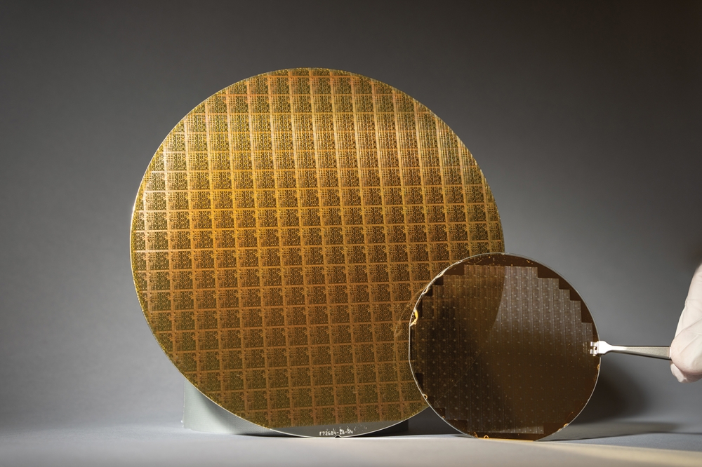
Could UV light improve semiconductor integration?

NREL scientists suggest that application of UV illumination could improve the optical properties of semiconductor layers
Integrating different semiconductor materials into an epitaxial device structure offers additional degrees of freedom to select for optimal material properties in each layer. However, interfaces between materials with different valences (i.e. III-V, II-VI and IV semiconductors) can be difficult to form with high quality.
Now, a discovery by Kwangwook Park and Kirstin Alberi, at the US Energy Department's National Renewable Energy Laboratory (NREL), suggests that careful application of UV illumination may be used to improve the optical properties of these material layers.
Park and Alberi experimented with integrating a layer of zinc selenide (ZnSe) grown on top of a layer of GaAs using UV light to modify the interface between them. Their results are published in a paper 'Tailoring Heterovalent Interface Formation with Light' in Scientific Reports.
Using a 150-watt xenon lamp to illuminate the growth surface, Park and Alberi determined the mechanisms of light-stimulated interface formation by varying the light intensity and interface initiation conditions. They found the UV light altered the mixture of chemical bonds at the interface through photo-induced desorption of arsenic atoms on the GaAs surface, resulting in a greater percentage of bonds between gallium and selenium, which help to passivate the underlying GaAs layer. The illumination also allowed the ZnSe to be grown at lower temperatures to better regulate elemental intermixing at the interface.
"The real value of this work is that we now understand how light affects interface formation, which can guide researchers in integrating a variety of different semiconductors in the future," Park said.
The work was funded by DOE's Office of Science.


