
Toshiba claims perovskite efficiency record
5-square centimetre multi-cell mini module delivers an energy conversion efficiency of 10.5 percent
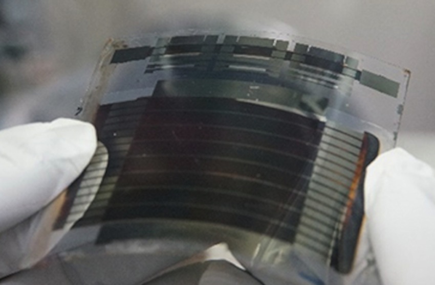
Toshiba has made a significant advance toward the realisation of light, flexible solar modules by fabricating a perovskite solar cell mini module with what it believes is the highest energy conversion rate yet achieved for such a device. The 5-square centimetre module delivers an energy conversion efficiency of 10.5 percent.
Toshiba achieved this advance by developing a fabrication process technology for film-based perovskite solar cells. The technology uses a film substrate and scribe process technology based on organic thin film solar cell module fabrication. Since this technology uses a flexible film substrate, it allows roll-to-roll fabrication that reduces costs. Toshiba will continue to refine the technology and expects to see further improvements in efficiency.
The results were presented at the New Energy and Industrial Technology Development Organisation (NEDO) meeting, held at the Pacifico Yokohama Annex Hall in Yokohama, Japan, on 22 September.
To date, there have been two main roadblocks to developing film-based perovskite solar cell modules: the difficulty of forming large, uniform perovskite polycrystalline layers; and the inability of the scribe process to remove the layer formed on top of the electrode - the flexibility of the film substrate prevents application of the strong blade pressure required for removal - which increases the resistance between cells and decreases conversion efficiency. As a result, modules formed on a film substrate have been difficult to fabricate and have had low conversion efficiency; there have been few reports on the technology.
Toshiba successfully applied a novel printing technology to fabrication of film-based perovskite solar cell modules, and achieved a 10.5 percent conversion efficiency in a 5X5cm module, the highest ever recorded.
Since this technology forms the substrate with a resin film, such as polyethylene terephthalate, a planar inverted structure (Figure 1) that can be fabricated at a temperature under 150deg is used for the cell structure. Toshiba addressed the problem of increasing the area by applying meniscus printing technology developed through R&D of organic thin film solar cells, and succeeded in forming a uniform thin layer of methylammonium lead iodide. This increased the efficiency of modules by reducing variation in properties between cells.
Toshiba's researchers also succeeded in increasing energy conversion efficiency by reducing the resistance between cells to the same level as with a glass substrate, through a combination of optimizing blade pressure during the scribe process, and also using materials that allow the layer covering the electrode to be removed even when blade pressure is weak. The reduced sheet resistance of the indium tin oxide transparent electrode developed for the resin substrate also contributed to increased efficiency.
Having demonstrated the possibility of increasing area and efficiency of a film-based module, and achieving a conversion efficiency of over 10 percent, Toshiba will now focus on increasing the module size and conversion efficiency, through measures including changing the composition of the perovskite material and by process improvements.


