Building a barrier against oxidation

Does Finnish start-up, Comptek Solutions, have a novel answer to the age-old problem of oxidation in compound semiconductors? Rebecca Pool takes a look.
A novel surface treatment is set to boost material quality in optoelectronic and RF devices.
In an industry development that could solve the thorny issue of oxidation in III-V compound semiconductors, Finland-based University of Turku spin-off, Comptek Solutions, has just won €450,000 to commercialise its novel surface treatment process.
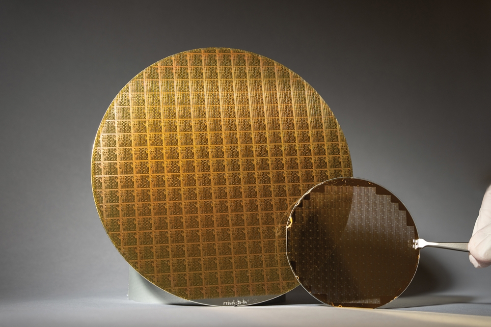
Designed to passivate the epi-layer surfaces that quickly oxidise when exposed to air, the process boosts material quality and is set to raise power efficiencies in optoelectronic and RF devices.
During semiconductor device fabrication, oxidation at III-V epi-layer surfaces leaves an amorphous layer riddled with electrically active defects. Some manufacturers employ cleaning techniques, from controlled chemical etching to in situ ion sputtering, to better prepare the semiconductor surface for later processing, but many players simply live with the problem and the less-than-ideal device performances that ensue.
"Industry has been trying to solve this problem, without success, for many, many years," highlights Comptek chief executive, Vicente Calvo Alonso. "But our treatment process represents a breakthrough with customers saying they get improved device performance, for instance in HEMT applications, as well as an increase in the number of amplifiers per wafer."
CEO, Vicente Calvo Alonso (left), CTO, Jouko Långe and Johnny Dahl, chief of research, (right).
Alonso and colleagues remain tight-lipped on detail, but describe 'Kontrox' as a passivation process based on novel atomic-level surface engineering that is fully compatible with MBE processes and can be implemented alongside other epitaxial methods.
Oxidised III-V surfaces are first cleaned, and then thermally oxidised in very precise conditions to produce a crystalline, almost defect-free, III-V oxide layer, ready for the next stages of fabrication. According to Alonso, the team has proven up to 98% reduction of defect state densities at technologically essential III-V dielectric interfaces.
Crucially, the improvement in crystal ordering at the surfaces as well as reduced defects enable manufacturers to narrow the gap between theoretical and practical device efficiencies. Meanwhile, better material homogeneity coupled with stability under air exposure boosts the manufacturing yields of subsequent processes.
"For example, side-wall passivation of III-Vs is a huge problem for laser manufacturers especially as wafers are moved from one process step to the next, and we have seen no practical solution yet," points out Alonso. "But we have optoelectronics manufacturers that are now willing to work with us in different applications and I believe this will be a huge breakthrough for them."
Comptek is now completing construction of its 40m2 state-of-the-art laboratory.
Optoelectronics manufacturing aside, Comptek is also seeing interest from the manufacturers of GaAs-based PHEMTs for power amplifiers in RF applications. As Comptek's chief technology officer, Jouko Lång, highlights: "Manufacturers want to deposit insulator materials on top of the III-V barrier layers before gate deposition, making a more CMOS type transistor structure called the MIS-HEMT."
"However, the insulator-III-V interface has been very poor so far and our process is a key enabler here," he adds. "Some of our customers have said they can gain up to 50% better transistor characteristics in their enhancement mode HEMTs when using our technology."
Spending plans
With its latest funds in tow, Comptek will complete construction of its 40m2 state-of-the-art laboratory, which will house a cleanroom, custom ultra-high-vacuum reactors and characterisation equipment. According to Alonso, the reactors are designed to handle wafer sizes up to four inches and produce high quality III-V-based structures.
"A few industry players are already fabricating chips on six inch wafers but many applications are still based on two and three inch wafers," says Alonso. "With our four inch capability, we will be able to work quickly with the evolving industry."
According to the chief executive, Comptex hopes to license its technology to epi-manufacturers, foundries and integrated device manufacturers, so will first provide samples and then work with customers to implement its process into production lines.
Comptek's passivation process is compatible with the majority of III-V compound materials.
"For molecular beam epitaxy reactors, implementation is pretty straightforward; our process is compatible with MBE and we are already in discussions with equipment manufacturers to develop equipment together," he says.
Here, Comptek will develop an 'add-on module' that can be quickly implemented to MBE reactors to perform the passivation process. Meanwhile, the company also intends to develop standalone equipment for MOCVD reactors.
"MOCVD is the industry's biggest market and we will be working with customers here on a case by case basis," says Alonso. "For example, as part of one request, we are looking at developing standalone equipment with a specific oxide removal process plus an atomic layer deposition capability."
"Introducing new processes to [users of ] MOCVD is going to take time but I am convinced that once the benefits of our process are known we will then be able to work with partners to speed up implementation," he adds.
Right now, Comptek's passivation process is compatible with the majority of III-V compound materials such as GaAs, InP, InAs, InSb and GaN. Customer sample production is the priority right now, but with good results already emerging, equipment development and implementation looks set to follow in the next year. And while the company currently comprises six employees, it is in the process of hiring and is already looking to its next round of venture capital funds.
"Industry has been trying to solve the oxidation problem for many years without success and our technology is giving very good results and interesting improvements," says Alonso. "We are already getting traction from industry and whenever we explain what we do, the interest is very big, which has to be a good sign."


