
2D photodetectors could improve solar energy efficiency
UC Riverside research invokes quantum mechanical processes that occur when two atomically thin materials are stacked together
Physicists at the University of California, Riverside have developed a photodetector by combining two distinct inorganic materials and producing quantum mechanical processes that could improve the way solar energy is collected.
Photodetectors are almost ubiquitous, found in cameras, cell phones, remote controls, solar cells, and even the panels of space shuttles. Increasing the efficiency of light-to-electricity conversion has been one of the primary aims in photodetector construction since their invention.
Lab researchers stacked two atomic layers of tungsten diselenide (WSe2) on a single atomic layer of molybdenum diselenide (MoSe2). Such stacking results in properties vastly different from those of the parent layers, allowing for customised electronic engineering at the tiniest possible scale.
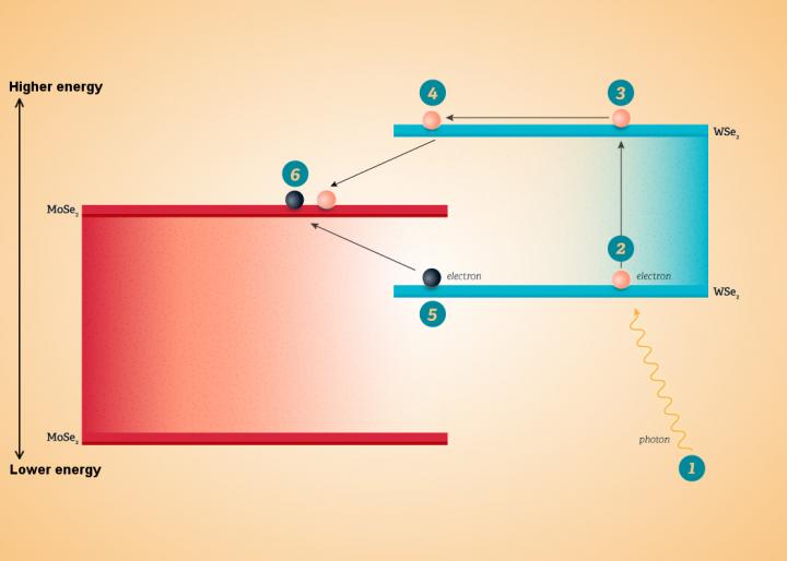
UC Riverside physicists observed that when a photon strikes the WSe2 layer, it knocks loose an electron, freeing it to conduct through the WSe2. At the junction between WSe2 and MoSe2, the electron drops down into MoSe2. The energy given off then catapults a second electron from the WSe2 into the MoSe2, where both electrons become free to move and generate electricity.
"We are seeing a new phenomenon occurring," said Nathaniel M. Gabor, an assistant professor of physics, who led the research team. "Normally, when an electron jumps between energy states, it wastes energy. In our experiment, the waste energy instead creates another electron, doubling its efficiency. Understanding such processes, together with improved designs that push beyond the theoretical efficiency limits, will have a broad significance with regard to designing new ultra-efficient photovoltaic devices." Study results appear in Nature Nanotechnology.
"The electron in WSe2 that is initially energised by the photon has an energy that is low with respect to WSe2," said Fatemeh Barati, a graduate student in Gabor's Quantum Materials Optoelectronics lab and the co-first author of the research paper. "With the application of a small electric field, it transfers to MoSe2, where its energy, with respect to this new material, is high. Meaning, it can now lose energy. This energy is dissipated as kinetic energy that dislodges the additional electron from WSe2."
In existing solar panels models, one photon can at most generate one electron. In the prototype the researchers developed, one photon can generate two electrons or more through a process called electron multiplication.
The researchers explained that in ultra-small materials, electrons behave like waves and the process of generating two electrons from one photon is perfectly allowable at extremely small length scales. "It's like a wave stuck between walls closing in," Gabor said. "Quantum mechanically, this changes all the scales. The combination of two different ultra small materials gives rise to an entirely new multiplication process. Two plus two equals five."
"Ideally, in a solar cell we would want light coming in to turn into several electrons," said Max Grossnickle, also a graduate student in Gabor's lab and the research paper's co-first author. "Our paper shows that this is possible."
Barati noted that more electrons could be generated also by increasing the temperature of the device.
"We saw a doubling of electrons in our device at 340 degrees Kelvin (150 F), which is slightly above room temperature," she said. "Few materials show this phenomenon around room temperature. As we increase this temperature, we should see more than a doubling of electrons."
Electron multiplication in conventional photocell devices typically requires applied voltages of 10-100 volts. To observe the doubling of electrons, the researchers used only 1.2 volts, the typical voltage supplied by an AA battery. "Such low voltage operation, and therefore low power consumption, may herald a revolutionary direction in photodetector and solar cell material design," Grossnickle said.
He explained that the efficiency of a photovoltaic device is governed by a simple competition: light energy is either converted into waste heat or useful electronic power. "Ultrathin materials may tip the balance in this competition by simultaneously limiting heat generation, while increasing electronic power," he said.
Gabor concluded: "These materials, being only an atom thick, are nearly transparent," he said. "It's conceivable that one day we might see them included in paint or in solar cells incorporated into windows. Because these materials are flexible, we can envision their application in wearable photovoltaics, with the materials being integrated into the fabric. We could have, say, a suit that generates power - energy-harvesting technology that would be essentially invisible."
Gabor, Barati and Grossnickle were joined in the study by UC Riverside's Shanshan Su, Roger K. Lake, and Vivek Aji.
The research was supported by grants from the Air Force Office of Scientific Research, US Department of Energy, a Cottrell Scholar Award, and a National Science Foundation CAREER Award.


