
Doped dots release laser light more efficiently
By adding extra charge carriers, Los Alamos team block absorption and create transparency without external stimulation
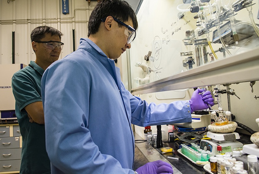
Los Alamos National Laboratory's Nanotech team has found a way to dope quantum dots with additional electrons to improve their efficiency in tiny laser devices such as opthalmic surgery scalpels.
"When we properly tailor the compositional profile within the particles during their fabrication, and then inject two or more electrons in each dot, they become more able to emit laser light. Importantly, they require considerably less power to initiate the lasing action," said Victor Klimov, leader of the Nanotech team.
In order to force a material to emit laser light one has to work toward a 'population inversion' in which the number of electrons in a higher-energy electronic state exceed the number that are in a lower-energy state. To achieve this condition normally, one applies an external stimulus (optical or electrical) of a certain power, which should exceed a critical value termed the optical-gain threshold. The Los Alamos researchers demonstrated that by adding extra electrons into their specially designed quantum dots, they can reduce this threshold to virtually zero.
A standard lasing material, when stimulated by a pump, absorbs light for a time before it starts to lase. On the way to lasing, the material transitions through the state of 'optical transparency' when light is neither absorbed nor amplified. By adding extra charge carriers to their quantum dots, the Los Alamos researchers were able to block absorption and create the state of transparency without external stimulation. This implies that even extremely weak pumping can now initiate lasing emission.
Another important ingredient of this research is a new type of quantum dots with their interiors designed to maintain the lasing-active state for much longer than standard particles do. Normally, the presence of extra electrons would suppress lasing because quantum dot energy is quickly released not as a photon stream but wasteful heat. The new Los Alamos particle design eliminates these parasitic losses, redirecting the particle's energy into the emission channel.
"These studies open exciting opportunities for realizing new types of low-threshold lasing devices that can be fabricated from solution using a variety of substrates and optical cavity designs for applications ranging from fibre optics and large-scale lasing arrays to laser lighting and lab-on-a-chip sensing technologies," Klimov said.
Funding: The work on the synthesis of graded quantum dots and studies of Auger recombination in synthesised materials was supported by the DOE Office of Science. The studies of the effect of charging on quantum dot optical gain properties were supported by the Laboratory Directed Research and Development (LDRD) program at Los Alamos National Laboratory.
'Towards zero-threshold optical gain using charged semiconductor quantum dots', by Kaifeng Wu et al; Nature Nanotechnology (2017) 16th October.


