
MIT team uses 2D materials to add optical comms on-chip
Ultrathin films of MoTe2 that emit and detect light can be stacked on top of silicon wafers
In a paper published in the journal Nature Nanotechnology, MIT researchers have described a light emitter and detector that can be integrated into silicon CMOS chips. The paper's first author is MIT postdoc Ya-Qing Bie, who is joined by Pablo Jarillo-Herrero and an interdisciplinary team including Dirk Englund, an associate professor of electrical engineering and computer science at MIT.
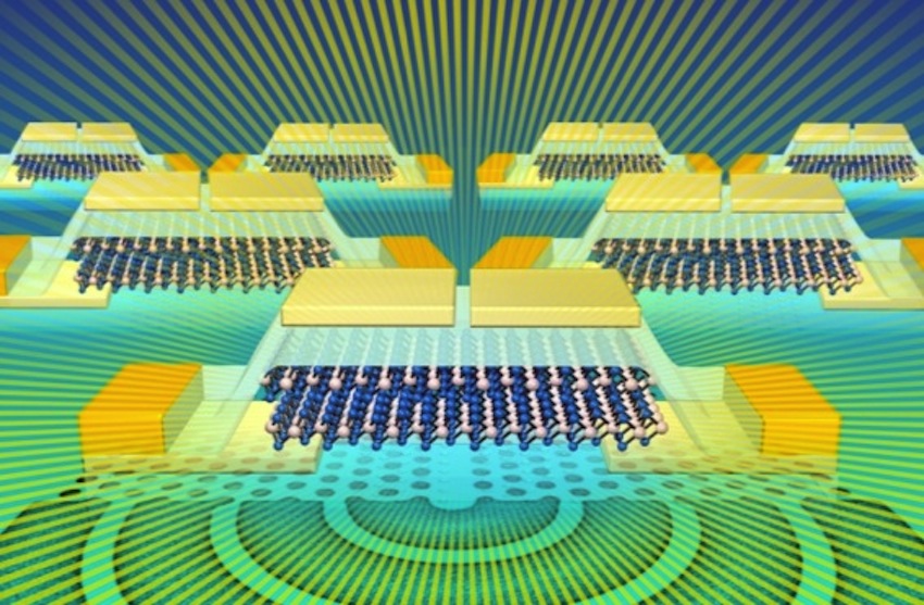
The device is built from the 2D compound semiconductor MoTe2, a transition-metal dichalcogenide. Unlike conventional semiconductors, the material can be stacked on top of silicon wafers, Jarillo-Herrero says.
"Researchers have been trying to find materials that are compatible with silicon, in order to bring optoelectronics and optical communication on-chip, but so far this has proven very difficult," Jarillo-Herrero says. "For example, GaAs is very good for optics, but it cannot be grown on silicon very easily because the two semiconductors are incompatible."
In contrast, the 2D MoTe2 can be mechanically attached to any material, Jarillo-Herrero says.
Another difficulty with integrating other semiconductors with silicon is that the materials typically emit light in the visible range, but light at these wavelengths is simply absorbed by silicon. MoTe2 emits light in the infrared range, which is not absorbed by silicon, meaning it can be used for on-chip communication.
To use the material as a light emitter, the researchers first had to convert it into a P-N junction diode, a device in which one side, the P side, is positively charged, while the other, N side, is negatively charged.
In conventional semiconductors, this is typically done by introducing chemical impurities into the material. With the new class of 2D materials, however, it can be done by simply applying a voltage across metallic gate electrodes placed side-by-side on top of the material.
"That is a significant breakthrough, because it means we do not need to introduce chemical impurities into the material [to create the diode]. We can do it electrically," Jarillo-Herrero says.
Once the diode is produced, the researchers run a current through the device, causing it to emit light. "So by using diodes made of MoTe2, we are able to fabricate LEDs compatible with silicon chips," Jarillo-Herrero says.
The device can also be switched to operate as a photodetector, by reversing the polarity of the voltage applied to the device. This causes it to stop conducting electricity until a light shines on it, when the current restarts. In this way, the devices are able to both transmit and receive optical signals.
The device is a proof of concept, and a great deal of work still needs to be done before the technology can be developed into a commercial product, Jarillo-Herrero says.
This paper fills an important gap in integrated photonics, by realising a high-performance silicon-CMOS-compatible light source, says Frank Koppens, a professor of quantum nano-optoelectronics at the Institute of Photonic Sciences in Barcelona, Spain, who was not involved in the research.
"This work shows that 2D materials and Si-CMOS and silicon photonics are a natural match, and we will surely see many more applications coming out of this [area] in the years to come," Koppens says.
The researchers are now investigating other materials that could be used for on-chip optical communication.
Most telecommunication systems, for example, operate using light with a wavelength of 1.3 or 1.5 micrometers, Jarillo-Herrero says. However, MoTe2 emits light at 1.1µm. This makes it suitable for use in the silicon chips found in computers, but unsuitable for telecommunications systems.
"It would be highly desirable if we could develop a similar material, which could emit and detect light at 1.3 or 1.5 micrometers in wavelength, where telecommunication through optical fibre operates," he says.
To this end, the researchers are exploring another ultrathin material called black phosphorus, which can be tuned to emit light at different wavelengths by altering the number of layers used. They hope to develop devices with the necessary number of layers to allow them to emit light at the two wavelengths while remaining compatible with silicon.
"The hope is that if we are able to communicate on-chip via optical signals instead of electronic signals, we will be able to do so more quickly, and while consuming less power," Jarillo-Herrero says.
'A MoTe2-based light-emitting diode and photodetector for silicon photonic integrated circuits', by Ya-Qing Bie et al; Nature Nanotechnology, October 2017


