
Kyma Demonstrates 200mm GaN-on-QST Templates
Company successfully transfers process for making high quality GaN to K200 HVPE tool
Kyma Technologies, a developer of wide bandgap semiconductor materials technologies, has used its new K200 hydride vapour phase epitaxy (HVPE) growth tool to produce high quality 200mm diameter GaN on QST (Qromis Substrate Technology) templates.
This follows the company's announcement in 2016 of its demonstration of 150mm diameter GaN on QST templates in partnership with Qromis (formerly Quora Technology) and its recent announcement of the commissioning of Kyma's K200 HVPE growth tool.
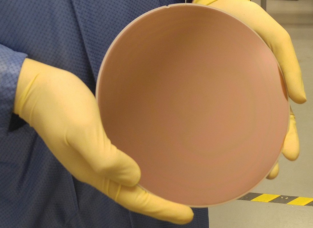
Pictured above one of the demonstrated 200mm diameter HVPE GaN on QST templates which consists of 10 microns of HVPE GaN grown on a 5 micron MOCVD GaN on QST wafer provided by Qromis.X-ray diffraction rocking curve line-widths for the templates fall in the range of 250 and 330 arc-sec for the symmetric {002) and asymmetric {102} XRD peaks, respectively, which is consistent with high structural quality. Low wafer bow (~50 microns) and smooth surface morphology suggest these materials should support high performance device manufacturing.
Kyma's newly constructed K200 HVPE tool is said to represent a first for the industry and was designed by Kyma engineers to enable uniform and rapid growth of high quality GaN on a number of different substrates.
"We have successfully transferred the process for making high quality GaN to our K200 HVPE tool. The structural quality of the GaN produced on Qromis' QST substrate is excellent. We are currently engaging with customers interested in large diameter GaN on QST templates," said Keith Evans, Kyma's president and CEO.
Kyma and Qromis are partnered for this work under a Kyma-led US DOE Phase IIB SBIR with award number DE-SC0009653.
Qromis recently began manufacturing 200mm QST substrates and GaN-on-QST wafers using its foundry partner Vanguard International Semiconductor (VIS). VIS is planning to offer GaN power device manufacturing services on 8-inch diameter QST platform in 2018.
Qromis co-founder and CEO Cem Basceri added: "Qromis' CMOS fab-friendly 200-mm diameter QST substrates and GaN-on-QST wafers represent a disruptive technology, enabling GaN epitaxy from a few microns to hundreds of microns for GaN power applications from 100V to 1,500V or beyond GaN power devices, in lateral, quasi vertical or vertical forms, on the same 8-inch or 12-inch production platform at Si power device cost. Kyma's K200 HVPE technology represents an important value-add to QST-based GaN power device manufacturing by enabling the low cost deposition of a thicker and lower defect density GaN surface than is practically achievable using MOCVD growth alone."
Kyma is also teamed with a world-class semiconductor equipment OEM to manufacture K200 HVPE tools for customers who prefer to bring Kyma's leading HVPE GaN growth process in-house.


