
Chip Combines Quantum Dot emitters and SiN Waveguides
New hybrid architecture could prove essential for high-performance quantum photonic circuits
Scientists at the US National Institute of Standards and Technology (NIST) and their collaborators have taken a step forward towards building quantum photonic circuits that rely on the quantum properties of light to process and communicate information rapidly and securely.
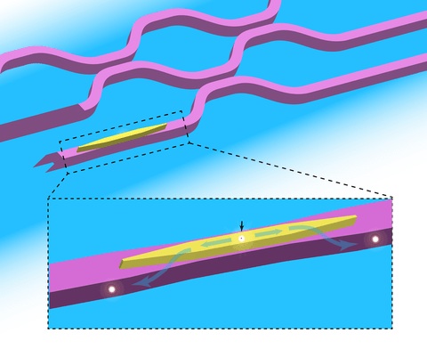
The quantum circuit architecture, developed by Marcelo Davanco and other NIST researchers along with collaborators from China and the UK, employs InAs/GaAs quantum dots to generate individual photons on the same chip as optical waveguides made from SiN.
To make the hybrid devices, Davanco and his colleagues first bonded two wafers together - one containing the quantum dots, the other containing the SiN waveguide material. They used a variation of a process that had originally been developed for making hybrid photonic lasers, which combined silicon for waveguides and compound semiconductors for classical light emission. Once the bonding was finished, the two materials were then sculpted with nanometer-scale resolution into their final geometries through state-of-the-art semiconductor device patterning and etching techniques.
Although this wafer bonding technique was developed more than a decade ago by other researchers, the team is the first to apply it towards making integrated quantum photonic devices.
"Since we have expertise in both fabrication and quantum photonics, it seemed clear that we could borrow and adapt this process to create this new architecture," notes Davanco.
The researchers say that the new architecture and the fabrication processes developed should enable them to reliably build larger circuits, which could perform more complex computations or simulations and translate into higher measurement precision and detection sensitivity in other applications.
The quantum dot employed by the team is a well-studied nanometer-scale structure: an island of the semiconductor InAs surrounded by GaAs. The InAs/GaAs nanostructure acts as a quantum system with two energy levels - a ground state (lower energy level) and an excited state (higher energy level). When an electron in the excited state loses energy by dropping down to the ground state, it emits a single photon.
Unlike most types of two-level emitters that exist in the solid state, these quantum dots have been shown to generate - reliably, on demand, and at large rates - the single photons needed for quantum applications.
In addition, researchers have been able to place them inside nanoscale, light-confining spaces that allow a large speedup of the single-photon emission rate, and in principle, could also allow the quantum dot to be excited by a single photon. This enables the quantum dots to directly assist with the processing of information rather than simply produce streams of photons.
The other part of the hybrid circuit architecture - passive waveguides made of SiN - are known for their ability to transmit photons across a chip's surface with very low photon loss. This allows quantum-dot-generated photons to efficiently coalesce with other photons at a beam splitter, or interact with other circuit elements such as modulators and detectors.
"We're getting the best of both worlds, with each behaving really well together on a single circuit," said Davanco. In fact, the hybrid architecture keeps the high performance achieved in devices made exclusively of each of the two materials, with little degradation when they are put together. He and his colleagues described the work in a recent issue of Nature Communications.
This work was performed in part at NIST's Center for Nanoscale Science and Technology (CNST), a shared-use facility available to researchers from industry, academia and government, and also included researchers from NIST's Physical Measurement Laboratory.
'Heterogeneous integration for on-chip quantum photonic circuits with single quantum dot devices' by M. Davanco et al; Nature Communications, 12 October 2017.


