Hybrid PICs target communication networks of tomorrow

Uniting III-Vs with silicon CMOS enables the fabrication of ground-breaking, low-cost lasers for access/metropolitan networks and datacentres by David Carrara and Guang-Hua Duan from III-V Lab and Segolene Oliver from CEA LETI
The last decade has witnessed an explosion in bandwidth demand on telecommunication and data communication networks. This has been driven by an uptake in smartphones, and the introduction of online services such as Youtube, Netflix, Google and Facebook. But this is just the beginning: 4k and 8k video streaming are the emerging new standards; data traffic for the smartphone will soon exceed that for the computer; and due to the growth of the Internet-of-Things, more objects are going to be connected to one another. Given this shift in the landscape, it is clear that bandwidth demands are going to increase drastically over the coming years, straining different layers within the communication networks.
Two of the key segments in this infrastructure are the datacentre and the access/metropolitan networks. The former deals with the data we "˜consume' from all over the world, while the latter provides links that allow us to access all that data from our homes and offices. In addition, access/metropolitan networks enable data transmission within a city or a local region.
Both the datacentre and the access/metropolitan networks are very different from long haul networks. They are much more sensitive to the cost, and the photonic components that are adopted have to be manufactured in far higher volumes.
To address this pair of requirements, the III-V Lab in Palaiseau, in partnership with CEA Leti in Grenoble, has developed a wafer-bonding approach that can form low-cost, efficient photonic integrated circuits (PICs) by uniting high-performance III-Vs with mature CMOS silicon. Armed with that approach for enabling the bonding of various types of III-V wafers on silicon, we have produced lasers that set a new benchmark for tunability and spectral purity, and fabricated the first silicon Mach Zehnder Modulator that is integrated with a tunable hybrid III-V/silicon laser.
Marrying two materials
At the heart of our approach is the marriage of the two main platforms in the semiconductor industry: silicon and III-V.
The former, the "˜mother' of modern electronics, is renowned for its really low cost, allied to it suitability for very large-volume production. But there is more to it than just that: silicon, working in tandem with its native oxide, can form compact passive optical elements with very good optical performances. Even modulators and detectors can be directly fabricated within this platform. However, one key component remains elusive "“ the laser.
Production of the laser is routine with a III-V semiconductor platform "“ and this can also be used to manufacture high-performance light detectors, modulators and amplifiers. However, these components have high production costs, due to smaller volumes within this industry and the less mature processes it employs.
By exploiting the advantages of both platforms, we have developed a hybrid technology that could unlock the door to the manufacture of low-cost, very high-performance PICs in high volume.
Device fabrication begins by taking 200 mm SOI wafers with a silicon top layer of typically 440 nm and using a hard mask technique to define different waveguide levels. A first partial etch of 220 nm, using a combination of deep UV lithography at 193 nm and reactive ion-etching, forms rib waveguides that are optimized for coupling with III-V waveguides "“ they are aligned on top of the silicon waveguides in a latter step. Additional etching steps form the passive circuitry, which includes strip waveguides, Bragg reflectors, filters and vertical-output couplers.
After physical structures were defined, selective dopant implantation creates p-n and p-i-n junctions in silicon and germanium. Finally, a high density plasma deposition process encapsulates the surface with an oxide. This oxide is planarized with a chemical-mechanical process to ensure a flat, smooth interface "“ a pre-requisite for a good molecular bonding with the III-V wafer. In parallel, we grow inverted III-V heterostructures on III-V substrates that have a diameter of either 2-inch, 3-inch or 4-inch. Optimised growth conditions ensure a defect-free surface that enables good quality wafer bonding and ultimately a high performance from the laser.
When working with InP-based semiconductors, the III-V region of our PICs consists of: a p-doped InGaAs contact layer; a p-doped InP cladding layer; typically six InGaAsP quantum wells, surrounded by two InGaAsP separate confinement heterostructure layers; and an n-doped InP layer. Molecular bonding unites these III-V wafers, epitaxial layer down, to the processed SOI wafers. Subsequent wet etching removes the III-V substrate, prior to laser dicing around the III-V wafers. This yields smaller wafers that are easier to process in a III-V fabrication plant.
Figure 1. The different steps used in the hybrid III-V/silicon process.
To define the different active sections of our III-V structure, we employ a combination of UV photolithography at 402 nm, selective wet etching, and reactive-ion etching with a mixture of hydrogen gas and methane (see Figure 1). Electrical contact pads and resistors are added by photolithography, followed by evaporation and sputtering of metals. After this we spin-coat a passivation layer of BCB, and then deposit a second metallic layer "“ an alloy of titanium, platinum and gold "“ to access the electrical pads through etched vias. Electro-optic characterisation of these components may be carried out directly on wafer, using the integrated vertical-grating couplers etched directly on the SOI wafers (see Figure 2).
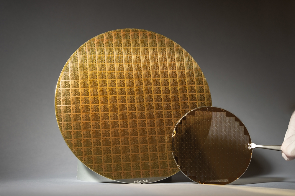
Figure 2. A wafer at the end of the III-V process (right) and a scanning electron microscopy cross-section of an active III-V section showing the alignment of the III-V waveguide and the silicon waveguide (left).
Access/metropolitain networks...
One potential application for our devices is in access networks. Today time-division multiplexing is used to create a data transmission rate of 1 Gbits/s, with just one wavelength shared between the users.But the future standard, NG-PON2, will incorporate wavelength-division multiplexing, by exploiting four wavelengths operating at 2.5-10 Gbits/s. Benefits of this move include a far higher bandwidth, enhanced flexibility and a new pricing policy.
A key element in every NG-PON2 network is a device that emits at different wavelength channels (up to 16 channels with 100 GHz channel spacing) and modulates light at 10 Gbits/s. As such a device will be embedded in each individual user internet box, rather than being shared by other users, it must be low in cost and available in high volume.
Figure 3. A hybrid III-V/silicon double ring laser provides temperature-dependent tuneable emission.
Our tuneable lasers fulfil these requirements (see Figure 3). They feature: an InP-based gain section, adiabatic tapers for the modal transfer between III-V and silicon waveguides; mirrors, etched in the SOI, on both sides of the cavity; and a double ring filtering system. By exploiting the Vernier effect, the two ring resonators can select a specific, unique Fabry Pérot mode of the cavity; and by heating the rings "“ by means of small metal heaters on the top of the ring resonators "“ the emission wavelength is easy to tune.
Top, Middle & Bottom: Figure 4. (a) Superimposed laser spectra for different currents injected into one heater, at 20°C. (b) Measured bit error rates for different lengths of fibre with a typical eye diagram for back-to-back 10 Gbits/s transmission. (c) Measured bit error rates for various wavelengths after 10 km of propagation in single-mode fibre under 21.4 Gbits/s non return-to-zero modulation.
These lasers break new ground, delivering a tunability over 45 nm combined with a side-mode suppression ratio in excess of 40 dB (see Figure 4(a)). Thanks to these attributes, the devices demonstrate good quality transmission up to 60 km at 10.3 Gbit/s, according to measurements with a 231-1 pseudorandom binary sequence (see Figure 4(b)). Shorten the transmission distance to 10 km, and ten wavelengths are possible at 21.4 Gbit/s (see Figure 4(c)).
Based on these results, it is clear to see that our hybrid III-V/silicon tuneable lasers have great potential for NG-PON2 networks. They meet the requirements for 2.5 Gbits/s, and they are close to fulfilling them at 10 Gbits/s. More importantly, according to published work, they are the only devices providing 16 wavelength channels with 100 GHz channel spacing. Note that a similar ring-resonator approach was also demonstrated for a tuneable receiver.
To enhance the modulation speed, we have pioneered integrated direct modulation of the laser section with an external silicon modulator. This allows us to realise operation at 25 Gbits/s by combining a tuneable hybrid III-V/silicon laser, which is similar to those previously described, with a silicon Mach Zehnder modulator and an optical output coupler (see Figure 5). Modulation efficiency, expressed as VÏ€LÏ€, is around 2.2 V.cm, while the 3 dB modulation bandwidth exceeds 15 GHz. These results showcase the potential of our hybrid III-V/silicon integration technology for fabricating low-cost, tuneable transmitters for metropolitan networks with advanced modulation formats.
Figure 5. Integrating a silicon Mach-Zehnder modulator with a hybrid III-V/silicon tuneable laser increases the modulation speed.
... and datacentres
Due to the dramatic increase in global data centre traffic "“ Cisco Systems expects it to more than treble between 2015 and 2020 "“ the Ethernet standard is expected to shift from 25 GbE to 100 GbE. The new standard could be accomplished by combining four transmitters, emitting at a different wavelengths and modulating at 25 Gbits/s.
To comply with this new standard, which will include a low cost requirement, we have developed a 4 x 25 wavelength-division multiplexing transmitter with our hybrid III-V/silicon process. This transmitter integrates four distributed feedback lasers, each emitting a different wavelength around 1.3 μm. Channel separation is 4.5 nm, corresponding to an 800 GHz wavelength-division multiplexing grid.
Figure 6. A 4x25 Gbits/s wavelength division multiplexing transmitter meets the requirements for 100 GbE.
Within these components, each laser is integrated with an electro-absorption modulator. A multi-mode interferometer coupler combines the light exiting all four modulators, and directs this into a unique output waveguide. Here power is increased with a semiconductor optical amplifier. A vertical coupler, etched at the end of the waveguide, enhances the output from this chip (see Figure 6).
Figure 7. An eye diagram of one arm of the wavelength-division multiplexing transmitter at 32 Gbits/s with an extinction ratio of 6.7 dB. This measurement showcases the potential of this technology for datacentre applications.
Using a pseudorandom binary sequence generator, this transmitter has produced bit error rates of just 10-9 and 5 x 10⁻⁵ at 25 Gbits/s and 32 Gbits/s, respectively. Under a modulation voltage of just 0.9 V peak-to-peak, and at a bias voltage of -0.6 V, the measured eye diagram is clearly opened at 32 Gbits/s (see Figure 7).
These results show that our III-V/SOI transmitter PICs are a promising solution for datacentres that require low-cost, high-volume integrated wavelength-division multiplexing transmitters operating at 100 Gbits/s. These devices, as well as those suitable for NG-PON2, demonstrate that our PICs can combine affordability with low energy consumption and a small footprint. As they are suitable for high-volume manufacture, they are excellent candidates for meeting the stringent needs of datacentre and access/metropolitan networks.


