
Kyma Demos 100mm Free-Standing GaN with Qromis
Kyma Technologies, a developer of wide bandgap semiconductor materials technologies, has announce it has produced its first 100mm diameter free-standing GaN substrates in partnership with Qromis, and benefiting from ARPA-E SWITCHES program support.
The 100mm diameter free-standing GaN substrate was produced in partnership with Qromis (formerly Quora Technology) who supplied a custom designed, low dislocation density GaN on QST (Qromis Substrate Technology) templates which Kyma used as the seed material for their HVPE GaN overgrowth.
This development was made possible with the financial support under the ARPA-E SWITCHES program. Kyma's original SWITCHES project was focused on HVPE growth of GaN on GaN seeds grown by ammonothermal growth technique. Lack of available high-quality large-diameter ammonothermally grown GaN seeds led Kyma to partner with Qromis and pivot its seed approach to one based on Qromis' innovative and disruptive QST materials platform which is scalable to 300mm diameter.
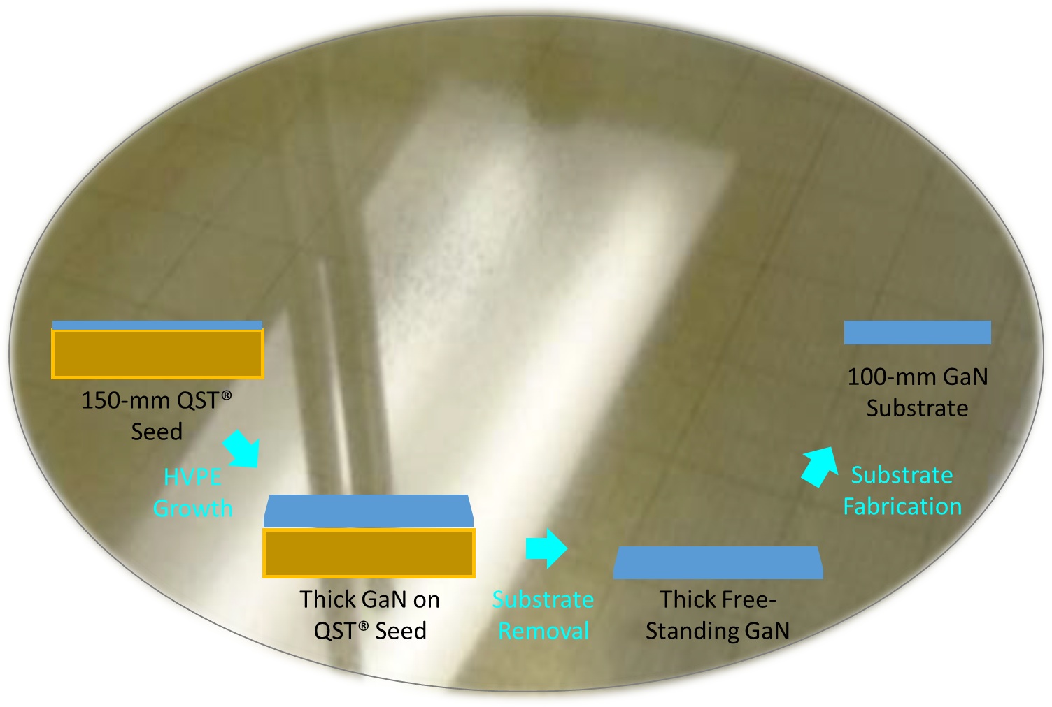
Pictured is one of the free-standing GaN wafers that was grown on and removed from a custom designed QST seed stack and then polished through CMP to create an epi-ready surface. The picture includes a simple description of the basic process steps used, beginning with the QST seed, growing thick GaN by HVPE, removing the QST seed stack to create thick large area free-standing GaN, and then fabricating to a final 100-mm diameter GaN substrate.
Kyma has developed several "special techniques" for managing the HVPE growth and the QST seed removal steps, and Qromis has developed a custom, high crystal quality GaN on QST template which served as a seed material.
Kyma president and CEO Keith Evans commented: "It is exciting to extend our partnership with Qromis to create large diameter free-standing GaN materials which can be further tailored as a new 100mm diameter GaN substrate offering. or used as seeds for GaN boule growth at Kyma. We are also bullish that our approach, which leverages the diameter scalability of both HVPE and Qromis' QST materials platform, can be extended to create 150-mm diameter GaN substrates in the near future and even 200-mm and larger GaN substrates over the longer term."
The Kyma and Qromis team has already demonstrated high-quality HVPE GaN template growth on both 150-mm and 200-mm diameter custom designed QST substrates.
Qromis co-founder and CEO Cem Basceri added: "We are pleased that Kyma was able to create large-area free-standing GaN materials using Qromis' patent-protected and CMOS fab-friendly GaN on QST wafers. as seed material. This specific achievement validates once again that QST technology will not only impact the performance and economies of scale for the existing, state of the art GaN devices but it will also enlarge the addressable markets and open up new applications."
Qromis recently began manufacturing 200-mm QST substrates and GaN-on-QST wafers using its foundry partner Vanguard International Semiconductor (VIS). VIS is planning to offer GaN power device manufacturing services on 8-inch diameter QST platform in 2018.


