VCSEL home run for IQE

Is IQE ready to supply the wafers that will take VCSELs to mass market, asks Rebecca Pool.
Just five days after the release of Apple's much-awaited iPhone 8, IQE revealed plans to make VCSELs a mass-market product by 2022.
The announcement came amid widespread media reports that the Wales-based wafer manufacturer was at the heart of the all-important VCSEL-driven facial recognition in Apple's latest incarnation.
As expected IQE remained dutifully tight-lipped on any links with the technology titan, sitting tight as share prices tripled to make it the second-best performer in the FTSE AIM 100 Index year-to-date.
Iwan Davies, group technology director at IQE, is pragmatic about IQE's latest success.
His company's photonics sector has experienced 'extremely rapid growth' largely thanks to VCSEL wafer sales; he expects sensing to be the largest application for some time; yet he is clear that IQE will supply wafers into any mass market application.
"There are industrial heating applications and many other consumer applications out there," he says. "We are ramping up production, have signed a lease on more manufacturing premises and are ordering new epitaxy tools."
"We expect rapid growth in this market and hopefully will be involved," he adds.
Modesty aside, Davies is very clear that IQE's VCSEL wafer success has been helped by the €23 million, EU-funded 'VIDaP' project.
In May 2014, 'VCSEL pilot pine for IR Illumination, Datacom and Power applications' set out to establish a pan-European supply chain capability for high volume VCSEL production, targeting infrared illumination, data communications, gesture recognition and industrial heating applications.
Led by Philips Technologie, Germany, the consortium included IQE, chip giant, STMicroelectronics, packaging equipment manufacturer, Sidel Blowing and Services of France, Germany-based industrial sensor maker, Sick, Israeli computer networking business, Mellanox Technologies, as well as Philips Electronics and the Technical University of Eindhoven, both from The Netherlands.
As Davies highlights: "At the time, we essentially had a very unstable process and had to employ experienced epitaxy engineers to oversee the process and use expertise to bring it up to a standard."
"This hands-on engineering monitoring process meant there could be a tendency to over-engineer the process, and we wanted to move away for this," he adds.
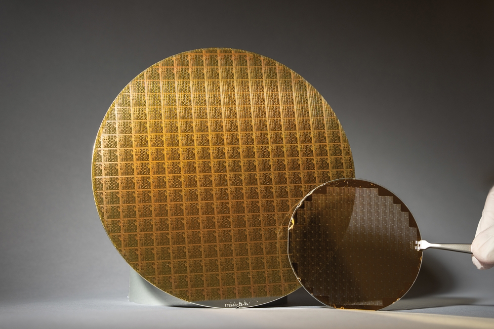
Fast-forward three years, and the project has established a fully automated production line for four inch GaAs wafers.
Manufacturing standards are said to match those of other high volume semiconductor processes. And Philips, which had been producing VCSELs on three inch wafers for many years, claims to have now produced more than 500 million devices in the last two years, up from 200 million across the previous decade. The company also claims to be ready to migrate to six inch wafer processes.
According to Davies, a key part of the project was understanding the dependence between IQE's epitaxy and device fabrication from Philips. Project researchers scrutinised materials characterisation data, such as luminescence and reflectance, alongside device performance parameters including output power, efficiency and emission wavelength.
From here, they developed an in-situ monitoring process to better control epitaxy processes, while state-of-the-art ex-situ characterisation equipment was used to check wafer specifications, after epitaxy.
Crucially, come the end of the project, the original Aixtron G3 reactor had been replaced by a G4 reactor, doubling wafer throughput per production run.
As Davies points out, the robust statistical process control system was critical to mapping control charts, minimising process drift and increasing wafer yields.
"Statistical process control, manufacturing execution systems and IT resources have all helped us to collect and compare data in a more statistical way, so we could move away from the hands-on engineering monitoring process," he emphasises.
As a result, the process now churns out the larger four inch wafers, more quickly, and in greater quantities per production.
Davies will not be drawn on absolute yield figures - simply stating yields are up by more than 25% - but emphasises the faster wafer processing speeds.
"The cycle time became a little shorter between runs as we gained more confidence in the stability of the process," he says. "So essentially we doubled wafer throughput in a run and also doubled the throughput per unit time."
"And given this is just after a year of running the new tools, we could have yet more wins, giving us an even higher throughput again," he adds.
Importantly project success comes just as industry analysts predict global VCSEL market revenues to mushroom from today's multi-million dollar levels to at least $1 billion in 2022.
A crucial part of the VIDaP project was to create mass market applications for VCSELs, and judging from the latest iPhone 8 developments, facial recognition in mobile phone handsets is a winner.
"Some of our end-user partners were extremely successful in using VCSELs; this is especially true in datacoms and 3D sensing applications," says Davies. "So we are ramping up production, have ordered five new Aixtron G4 reactors giving us fourteen [reactors], with our new site having the capacity for 100 such tools."
"The exploitation of VIDaP is clearly already there to be seen," he adds.


