Loading...
News Article

Random light patterns - a novel cyber security solution?

News

US team develops new class of cybersecurity primitives around the structural randomness of 2D semiconductor MoS2

Researchers at New York University Tandon School of Engineering have developed a new class of unclonable cybersecurity security primitives using the high level of structural randomness in 2D MoS2 .

Randomness is highly desirable for constructing the security primitives that encrypt and thereby secure computer hardware and data physically, rather than by programming.

In a paper published in the journal ACS Nano ('Physically Unclonable Cryptographic Primitives by Chemical Vapor Deposition of Layered MoS2), Davood Shahrjerdi and his NYU Tandon team offer the first proof of complete spatial randomness in atomically thin MoS2.

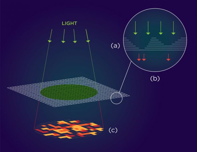
The researchers grew the nanomaterial in layers. By varying the thickness of each layer, Shahrjerdi explained, they tuned the size and type of energy band structure, which in turn affects the properties of the material.

"At monolayer thickness, this material has the optical properties of a semiconductor that emits light, but at multilayer, the properties change, and the material no longer emits light. This property is unique to this material," he said.

By tuning the material growth process, the resulting thin film is speckled with randomly occurring regions that alternately emit or do not emit light. When exposed to light, this pattern translates into a one-of-a-kind authentication key that could secure hardware components at minimal cost.

Shahrjerdi said his team was pondering potential applications for what he described as the beautiful random light patterns of MoS2 when he realised it would be highly valuable as a cryptographic primitive.

This is though to represent the first physically unclonable security primitive created using this nanomaterial. Typically embedded in integrated circuits, physically unclonable security primitives protect or authenticate hardware or digital information. They interact with a stimulus - in this case, light - to produce a unique response that can serve as a cryptographic key or means of authentication.

The research team envisions a future in which similar nanomaterial-based security primitives can be inexpensively produced at scale and applied to a chip or other hardware component, much like a postage stamp to a letter. "No metal contacts are required, and production could take place independently of the chip fabrication process," Shahrjerdi said. "It's maximum security with minimal investment."

SPONSOR MESSAGE

Secure Your Hydrogen Supply

A study supply of high-purity hydrogen is critical to semiconductor fabrication. Supply chain interruptions are challenging manufacturers, leading to production slowdowns and stoppages. On-site hydrogen generation offers a scalable alternative for new and existing fabs, freeing the operator from dependence on delivered gas.

Plant managers understand the critical role that hydrogen plays in semiconductor fabrication. That important job includes crystal growth, carrier gas, wafer annealing, and in the emerging Extreme UV Lithography (EUV) that will enable new generations of devices. As the vast need for semiconductors grows across all sectors of world economies, so does the need for high-purity hydrogen.

Take control with Nel on-site hydrogen generation.

Read more
Say hello to the heterogeneous revolution
Double heterostructure HEMTs for handsets
AlixLabs to collaborate with Linköping University
SiC MOSFETs: Understanding the benefits of plasma nitridation
Wolfspeed reports Q2 results
VueReal secures $40.5m to scale MicroSolid printing
Mitsubishi joins Horizon Europe's FLAGCHIP project
Vishay launches new high voltage SiC diodes
UK team leads diamond-FET breakthrough
GaN adoption at tipping point, says Infineon
BluGlass files tuneable GaN laser patents
QD company Quantum Science expands into new facility
Innoscience files lawsuit against Infineon
Riber revenues up 5% to €41.2m
Forvia Hella to use CoolSiC for next generation charging
Photon Design to exhibit QD simulation tool
Ortel transfers CW laser fabrication to Canada
Luminus adds red and blue multi-mode Lasers
PseudolithIC raises $6M for heterogeneous chiplet tech
Mesa sidewall design improves HV DUV LEDs
IQE revenue to exceed expectations
'Game-changing' VCSEL system targets clinical imaging
German start-up secures finance for SiC processing tech
Macom signs preliminaries for CHIPS Act funding
IQE and Quintessent partner on QD lasers for AI
EU funds perovskite tandems for fuel-free space propulsion
EU to invest €3m in GeSi quantum project
Transforming the current density of AlN Schottky barrier diodes
Turbocharging the GaN MOSFET with a HfO₂ gate
Wolfspeed launches Gen 4 SiC MOSFET technology
Report predicts high growth for UK's North East
Element Six unveils Cu-diamond composite
×
Search the news archive

To close this popup you can press escape or click the close icon.
Logo
x
Logo
×
Register - Step 1

You may choose to subscribe to the Compound Semiconductor Magazine, the Compound Semiconductor Newsletter, or both. You may also request additional information if required, before submitting your application.


Please subscribe me to:


You chose the industry type of "Other"

Please enter the industry that you work in:
 
x
Adblocker Detected
Please consider unblocking adverts on this website