
Ga-doping achieves Record Low Contact Resistivity
Imec's Ga-doped Ge-rich source/drain contacts are promising for suppressing parasitic source/drain resistance in advanced pMOS devices
At this week's 2017 International Electron Devices Meeting (IEDM), Imec, the research and innovation hub, reports ultralow contact resistivity of 5x10⁻¹⁰Ωcm2 on Gallium-doped p-Germanium source/drain contacts.
The low contact resistivity and high level of Ga activation were achieved after nanosecond laser activation (NLA) at low thermal budget. The results show that highly Ga-doped Ge-rich source/drain contacts provide a promising route for suppressing parasitic source/drain resistance in advanced pMOS devices.
These breakthrough results are important in light of further downscaling of the CMOS source/drain contact area, which is challenged by a parasitic source/drain resistance and results in suboptimal transistor functioning.
High dopant activation is known to be an attractive approach for lowering source/drain contact resistance. Traditionally in pMOS devices, Silicon (Si) source/drain contacts with high boron (B) activation are used.
But in more advanced pMOS devices, Ge- and SiGe(Sn)-based source/drain are a promising alternative since they introduce beneficial strain. However, the higher the Ge content, the lower the boron activation and solubility in Ge or Ge-rich SiGe.
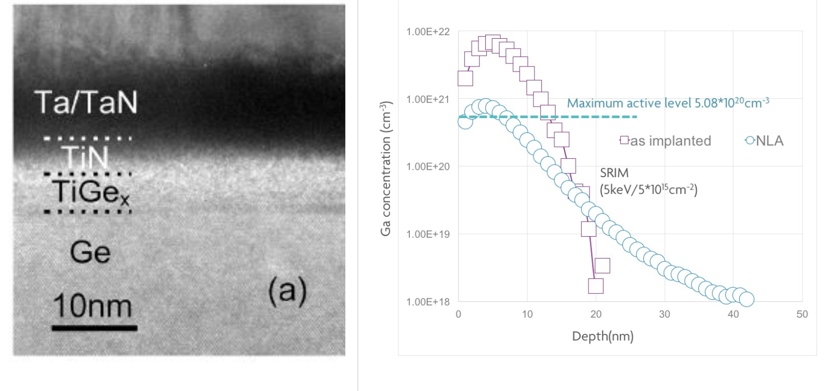
The new findings result from a comprehensive study of Ga dopant activation in Si, Si0.4Ge0.6 and Ge conducted by Imec, KU Leuven (Belgium) and Fudan University (Shangai, China). In this study, either rapid thermal annealing (RTA) or Applied Materials' nanosecond laser activation (NLA) were used as dopant activation technologies, after Ga ion implantation. A record low contact resistivity of 5x10⁻¹⁰Ωcm2 and a high dopant activation level of 5x1020cm-3 were obtained for Ga-doped Ge source/drain contacts after NLA.
The low contact resistivity can be attributed to a beneficial Ge/Ga surface aggregation following the NLA process. With RTA activation at 400degC, a contact resistivity as low as 1.2x10⁻⁹Ωcm2 was reported. The study shows that Ga might be preferred over B as a dopant for Ge or high-Ge content source/drain contacts in pMOS devices.
"For the first time, we have achieved contact resistivities far below 10-9Ωcm2 for high-Ge content source/drain contacts," said Naoto Horiguchi, distinguished member of the technical staff at Imec. "This proves that Ga doping and activation by NLA or RTA are an attractive alternative to boron doping for these source/drain contacts. It provides a possible path for further performance improvement using the current source/drain schemes in next-generation technology nodes."
The results were obtained at low thermal budget activation, making Ga doping particularly attractive for devices that require low-thermal budget processing.
Imec's research into advanced logic scaling is performed in cooperation with key CMOS program partners including GlobalFoundries, Huawei, Intel, Micron, Qualcomm, Samsung, SK Hynix, SanDisk/Western Digital, Sony Semiconductor Solutions, TOSHIBA Memory and TSMC.
Figure: Ga implanted in Ge and activated by NLA: (left) TEM image and (right) SIMS profile and calculated active carrier concentration level.


