
US researchers make flexible GaN chips
Air Force Research Laboratory researchers use boron nitride to transfer GaN circuits to flexible substrates
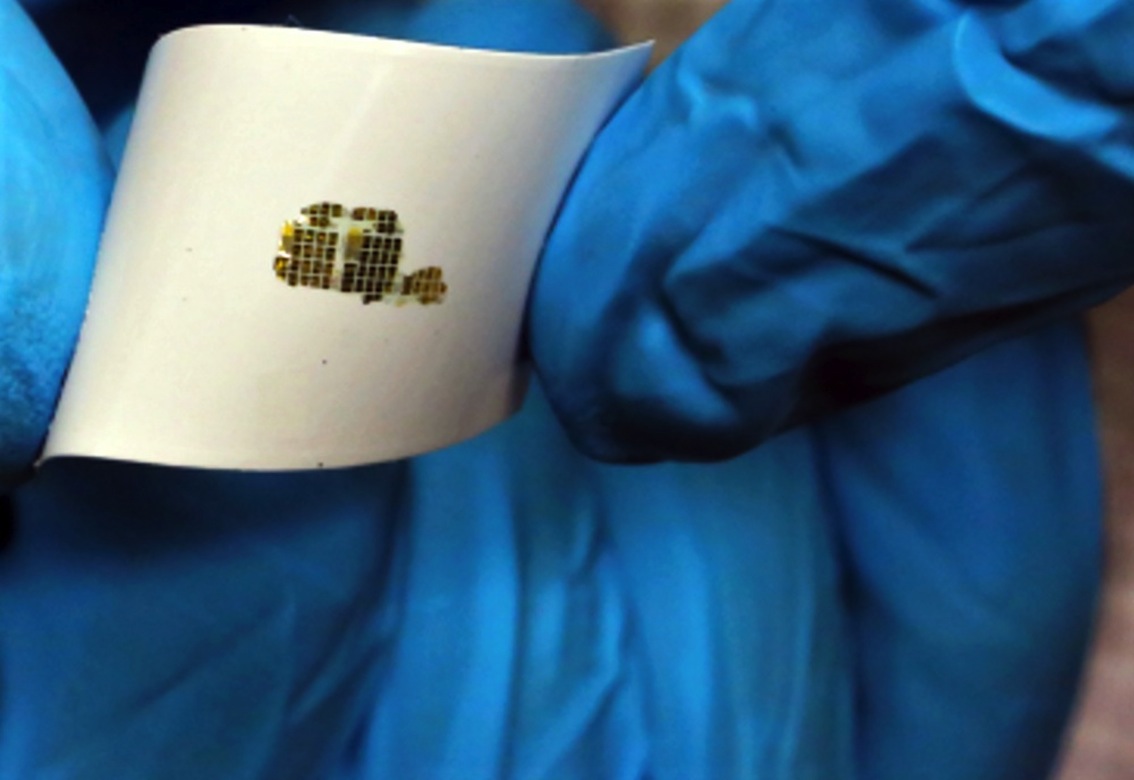
Scientists at the US Air Force Research Laboratory have discovered a new way to grow and transfer GaN onto a flexible substrate, laying the groundwork for 5th generation, high speed, agile communication systems of the future.
"GaN is the basis for a lot of communication devices and is often used in high performance amplifiers or as a component of a radar or wireless system," said Nicholas Glavin, a research scientist at the AFRL Materials and Manufacturing Directorate. "We demonstrated the ability to grow and place the material on a flexible substrate, enabling the potential to power wearable devices or electronic devices that are not necessarily flat. We are the first group ever to demonstrate a flexible RF (radio frequency) transistor device based on GaN that actually performs under strain and is flexible, which is quite powerful."
At present, GaAs is often the material of choice for wireless devices. However it is limited in its ability to transmit high frequency signals at high power. This can cause data degradation or slow speeds of transfer at high range.
By contrast GaN has an exceptional ability to transmit large amounts of information at a high frequency with high power. Yet, it has been limited in application due to the high cost of material manufacturing, which typically requires a rigid substrate such as sapphire and precise thermal and chemical stability. Additionally, once grown on a substrate, the GaN made this way could only be used in flat, planar platforms, unable to withstand bending or strain.
The new AFRL method of GaN production takes advantage of the physical properties of boron nitride. Scientists grow the GaN on the BN, and then due to weak chemical bonds between the BN and the growing surface, they can then lift and transfer the apparatus to another substrate, enabling communication capability on unique platforms and devices.
"It's been a big DoD priority to further develop this material. We are the first to demonstrate a flexible RF transistor device using GaN that maintains high quality performance under strain using the transfer method," said Donald Dorsey, the lead for the Agile Radio Frequency Electronic Materials and Processes Team. "We now have the potential to create high frequency transmitters for high power communications and radar that use GaN in a more compact and versatile form. This is a tremendous advance in the science."
The ability to transfer the GaN to a flexible or other arbitrary substrate has tremendous value for the Air Force as communication needs continue to grow and expand at a rapid rate.
"There are two primary applications we see this research directly benefitting the Air Force," said Glavin. "The first is in wearable systems -- as we collect more information on our operators and develop more sensor technologies, we need to be able to take that information and communicate it for action. A flexible transmitter based on GaN can make this happen more efficiently. Another area that will benefit is flexible and conformal radar technology. Typical radar systems are big and bulky, but using this technology we can create systems that can be more easily integrated into dynamic environments."
Another benefit is power amplification directly on antenna systems, said Michael Snure, a senior physicist at the AFRL Sensors Directorate.
"If you have a flexible power amplifier and can get it as close as possible to your radar antenna, you can improve performance simply by removing the distance a signal has to travel. Flexible GaN gets you the ability to place the amplifier up against the antenna on the same platform and improve performance and transmission," Snure said.
Though research continues to optimise the ability for the AFRL-developed GaN to integrate with diverse material surfaces and to find ways to improve performance and the transfer process, the team is already in the process of obtaining patents for both the material growth process and for the use of GaN in flexible RF devices.
"We performed the demo state and are now focusing on material integration," said Glavin. "This is a significant technological breakthrough, and it's even more important since 100 percent of the expertise behind it comes from AFRL. We are impacting communication for the future."
The AFRL team's research recently published in Advanced Materials with the title, 'Flexible GaN for High-Performance, Strainable Radio Frequency Devices.'


