
Leti integrates hybrid III-V lasers on CMOS
CMOS compatibility with silicon photonics lowers fabrication costs and provides access to mature and large-scale facilities
Leti, a research institute of CEA Tech in Grenoble, France, has integrated hybrid III-V silicon lasers on 200mm wafers using standard CMOS process flow. The results were reported December 5th at IEDM 2017 in a paper titled "Hybrid III-V/Si DFB Laser Integration on a 200mm Fully CMOS-compatible Silicon Photonics Platform".
Leti says this breakthrough shows a way forward for the industry to move away from 100mm wafers and bulk III-V technology.
CMOS compatibility with silicon photonics lowers fabrication costs, and provides access to mature and large-scale facilities, which enables packaging compatibility with CMOS driving circuits.

"Silicon-photonic technologies are becoming more mature, but the main limitation of these platforms is the lack of an integrated light source," said Bertrand Szelag, a co-author of the paper. "This project showed that a laser can be integrated on a mature silicon-photonic platform with a modular approach that does not compromise baseline process performances. We demonstrated that the entire process can be done in a standard CMOS fabrication line with conventional process and materials, and that it is possible to integrate all the photonic building blocks at large scale."
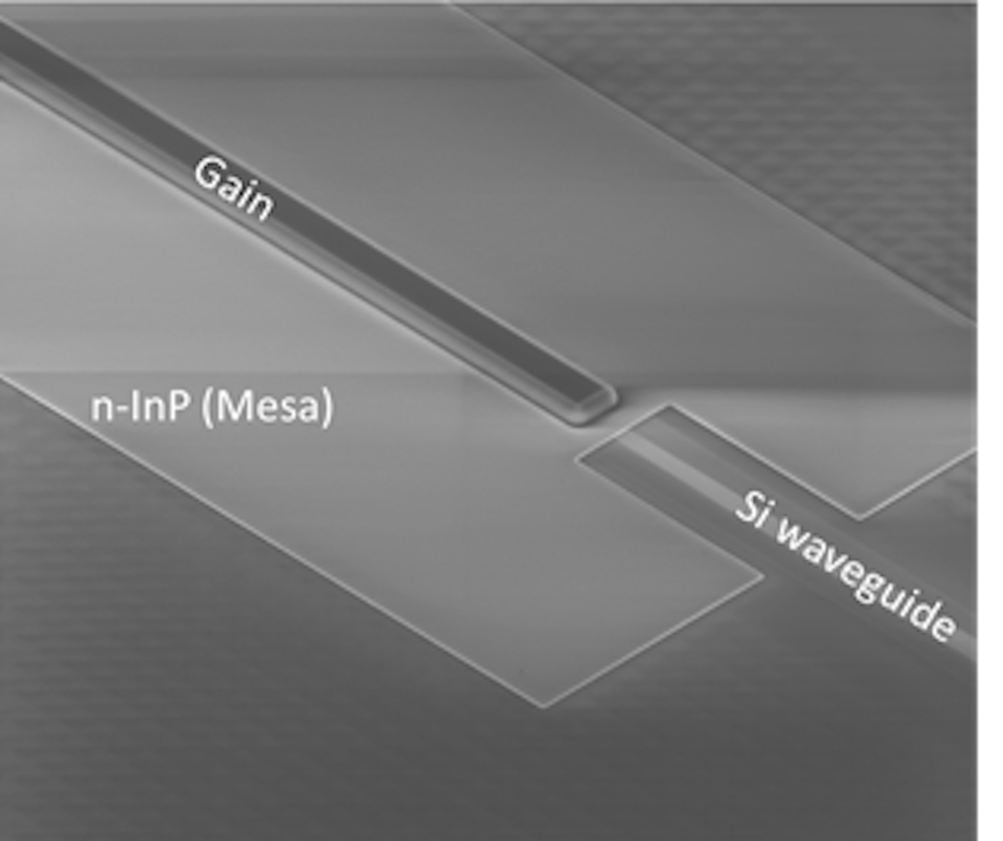
The integration required managing a thick silicon film, typically 500nm thick, for the hybrid laser, and a thinner one, typically 300nm, for the baseline silicon-photonic platform. This required locally thickening the silicon by adding 200nm of amorphous silicon via a damascene process, which presents the advantage of leaving a flat surface favourable for bonding III-V silicon.
The laser can be integrated on a mature silicon photonic platform with a modular approach that does not compromise the baseline process performance. (The graph above shows the laser spectrum at 160 mA injection currents).
The novelty of the approach also included using innovative laser electrical contacts that do not contain any noble metals, such as gold. The contacts also prohibit integration lift-off-based processes. Nickel-based metallisation was used with an integration technique similar to a CMOS transistor technique, in which tungsten plugs connect the device to the routing metal lines.
Next steps include integrating the laser with active silicon-photonic devices, e.g. a modulator and photodiode with several interconnect metal levels in a planarised backend. Finally, III-V die bonding will replace III-V wafer bonding in order to process lasers on the entire silicon wafer.


