
Tokyo University chooses EVG system for compound semi research
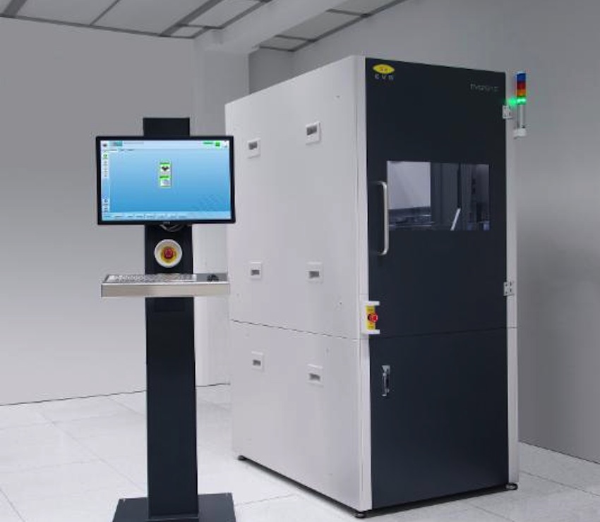
EVG810LT plasma activation system enables low-temperature direct wafer bonding of III-V materials and germanium-on-silicon wafers
EV Group (EVG), a supplier of wafer bonding and lithography equipment for MEMS, nanotechnology and semiconductors, has received an order from the University of Tokyo for its EVG810LT plasma activation system for compound semiconductor research.
Installed at the university's Takagi & Takenaka Laboratory, the EVG810LT augments the laboratory's research focused on developing novel MOSFET and electronic-photonic integrated circuits (EPICs) using III-V-on-insulator (III-V-OI) and germanium-on-insulator (GeOI) substrates.
These advanced material substrates are designed to exceed the performance of conventional silicon semiconductors as well as silicon photonics, where III-V materials such as InP, InGaAs and germanium are bonded to silicon wafers.
The EVG810LT activates a wafer surface using plasma for low-temperature direct wafer bonding, and has been used by other customers in high-volume manufacturing of silicon-on-insulator (SOI) wafers and backside illuminated CMOS image sensors.
The EVG810LT LowTemp Plasma Activation System from EV Group is ideal for direct bonding for manufacturing of silicon-on-insulator (SOI) strained silicon and germanium-on-insulator (GeOI) wafers as well as for compound semiconductor applications and MEMS devices.
"The miniaturisation of semiconductor devices is reaching its physical limitations, and shrinking transistor (scaling) in line with Moore's Law is not sufficient enough to address future demands for higher performance of LSI devices," noted Mitsuru Takenaka, associate professor at the Takagi & Takenaka Laboratory with the University of Tokyo.
"3D integrated circuits with III-V compound semiconductors or germanium stacked freely on silicon semiconductors are expected to be among the breakthroughs to enhance the performance of the LSIs after the end of Moore's Law. In support of our efforts, we adopted EV Group's plasma activation system, the EVG810LT, to help us achieve lower temperature and high-quality wafer bonds."
Commenting on today's announcement, Hiroshi Yamamoto, representative director of EV Group Japan K.K., said: "It is a great honour that our system was selected to support the University of Tokyo's leading-edge LSI device research. The innovative results at The Takagi & Takenaka Laboratory are expected to address the fundamental issues that the semiconductor industry currently faces. Based on our company's Triple-i philosophy of 'invent, innovate and implement', EV Group has been working with universities and R&D facilities that are active in advanced fields. We will continue to provide the Takagi & Takenaka Laboratory with the technical support they need to succeed with their leading-edge research."
The emergence of the Internet of Things (IoT), Big Data and artificial intelligence (AI) is driving a new wave of demand for electronic devices with lower power consumption, higher performance, and greater functionality. To meet this demand, the semiconductor industry is evaluating the benefits of incorporating new materials with silicon-beyond pure silicon-based wafers.
This shift is paving the way for future market growth of compound semiconductors, as well as more efficient manufacturing technologies to achieve maximum end-device performance. For example, MOCVD processes, where a thin film of II-VI or III-V material is deposited on a substrate by heteroepitaxial growth, can result in inconsistent wafer formation. This compromises the integrity of the wafer surface and ultimately impacts end-device performance. Direct wafer bonding with plasma activation is a promising solution to enable heterogeneous integration of different materials and to realise high-quality engineered substrates.
EVG will show the EVG810LT system at the SEMICON Japan exhibition being held December 13-15 at the Tokyo Bit Sight - Tokyo International Exhibition centre in Tokyo, Japan.


